Samsung Foundry to Almost Double Output by 2026
by Dr. Ian Cutress on October 6, 2021 1:00 PM EST- Posted in
- Samsung
- EUV
- Fab
- Samsung Foundry
- SFF2021
It’s hard not to notice that we’re in the middle of a semiconductor crunch right now. Factories are running at full steam, but pinch points in the supply chain are causing chaos and bottlenecks – whether that means not enough packaging materials, the cost of shipping has increased 10x, or additional tariffs, it’s causing various industries that rely on semiconductors to wait for supply and then pay over expected prices. Nonetheless, everything that is made is being sold, and so all of the big foundries are driving more investment into their supply chain ecosystem as well as raw manufacturing, and Samsung is no different.
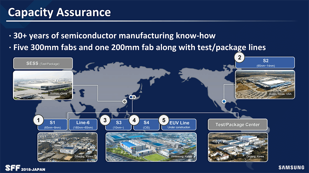
Samsung Foundry, as one of the three leading edge foundry offerings on the market, has the same message as the others: invest in production, invest in the supply chain, and offer a wider array of features that customers require. For example, the company announced earlier this year that it plans to spend USD$17 Billion on new manufacturing facilities in the USA by Late 2023, bolstering its US manufacturing beyond the 65nm/14nm S2 facility in Austin (the exact location of the new USA fab is unknown). Samsung also has 4 other fabs in Korea, along with testing and packaging facilities.
As part of the Samsung Foundry Forum 2021 event this week, the company is projecting an almost 2x increase in its wafer output from 2021 to 2026. Using 2017 as a starting point, Samsung states that through the production of its S3/S4 fabs and the first phase of its S5 fab coming online, it currently sits at 1.8x production of the 2017 number. By 2026, as S5 ramps and expands into its second phase, it expects to be around 3.2x (or more) than the 2017 output.
Samsung won’t let us recreate the slide in our briefing, but here are the salient points:
- 2017: 1.0x, S3/S4 Fabs start
- 2021: 1.8x, S5-Phase 1 Begins, Phase 2 in 2022/2023
- 2026: >3.2x
Samsung Foundry calls this their mid-term capacity plan. Right now Samsung has the following facilities:
- S1, Giheung Korea, for 8-65nm, Line 6 for 65-180nm
- S2, Austin USA, for 14-65nm
- S3, Hwaseong Korea, for 10nm-class
- S4, Hwaseong Korea, for CMOS Image Sensors
- S5, Hwaseong Korea, Phase 1 for EUV
- A Test/Package Center in Onyang, Korea
- A Test/Package Center in Suzhou, China
Between now and 2026 Samsung is expanding S5 into phase two as well as constructing the second fab in the USA. When asked for details about the new USA fab, we were told that no new information is coming out at this event, and to wait for further announcements and developments.


6 Comments
View All Comments
yamheychoco - Thursday, October 7, 2021 - link
https://biz.chosun.com/site/data/html_dir/2021/01/...The s5 is not a factory in Hwaseong. The foundry line included in Pyeongtaek P2 is S5. The Hwaseong EUV line is called V1.
https://biz.chosun.com/site/data/html_dir/2021/01/...
'Pyeongtaek Campus Foundry (S5)'
Ian Cutress - Thursday, October 7, 2021 - link
Just going from the picture embedded in the article, direct from Samsung in 2019yamheychoco - Thursday, October 7, 2021 - link
In 2019, the s5 line did not exist, and there may not have been an official name for the Hwasong EUV line. It is an image created simply to mean the 5th foundry line.Samsung Electronics is officially calling the Hwaseong EUV line V1. The same goes for the S5 line.
The following is quoted from the press release and conference call on Samsung Electronics Korea website.
[삼성전자가 화성사업장에 반도체 미래를 이끌 최첨단 EUV(Extreme Ultra Violet, 극자외선) 전용 라인인 ‘V1 라인’을 본격적으로 가동하고 ‘반도체 비전 2030’ 달성에 나섰다.]
[시스템 반도체는 스마트폰 성수기 진입에 따른 시스템LSI 주요 제품 수요 증가가 예상되는 가운데, 파운드리는 평택 S5 라인의 공급능력 확대 및 미래 투자 기반 마련을 위한 공급가격 현실화를 통해 성장을 가속할 것이다.]
https://news.samsung.com/kr/%EC%82%BC%EC%84%B1%EC%...
http://www.thelec.kr/news/articleView.html?idxno=1...
yamheychoco - Thursday, October 7, 2021 - link
https://samsungfoundry.com/foundry/homepage/anonym...Even on the updated Samsung Foundry English website, there is no number '5' on the Hwaseong EUV line.
dotjaz - Thursday, October 7, 2021 - link
You know it's funny when your own colleague reported the actual name and you didn't know about it.https://www.anandtech.com/show/15538/samsung-start...
dotjaz - Thursday, October 7, 2021 - link
Also according to Samsung's press release, no S5https://news.samsung.com/global/samsung-electronic...