Hot Chips 2018: Going Deep on NVSwitch Live Blog (8:45am PT, 3:45pm UTC)
by Ian Cutress on August 21, 2018 11:40 AM EST
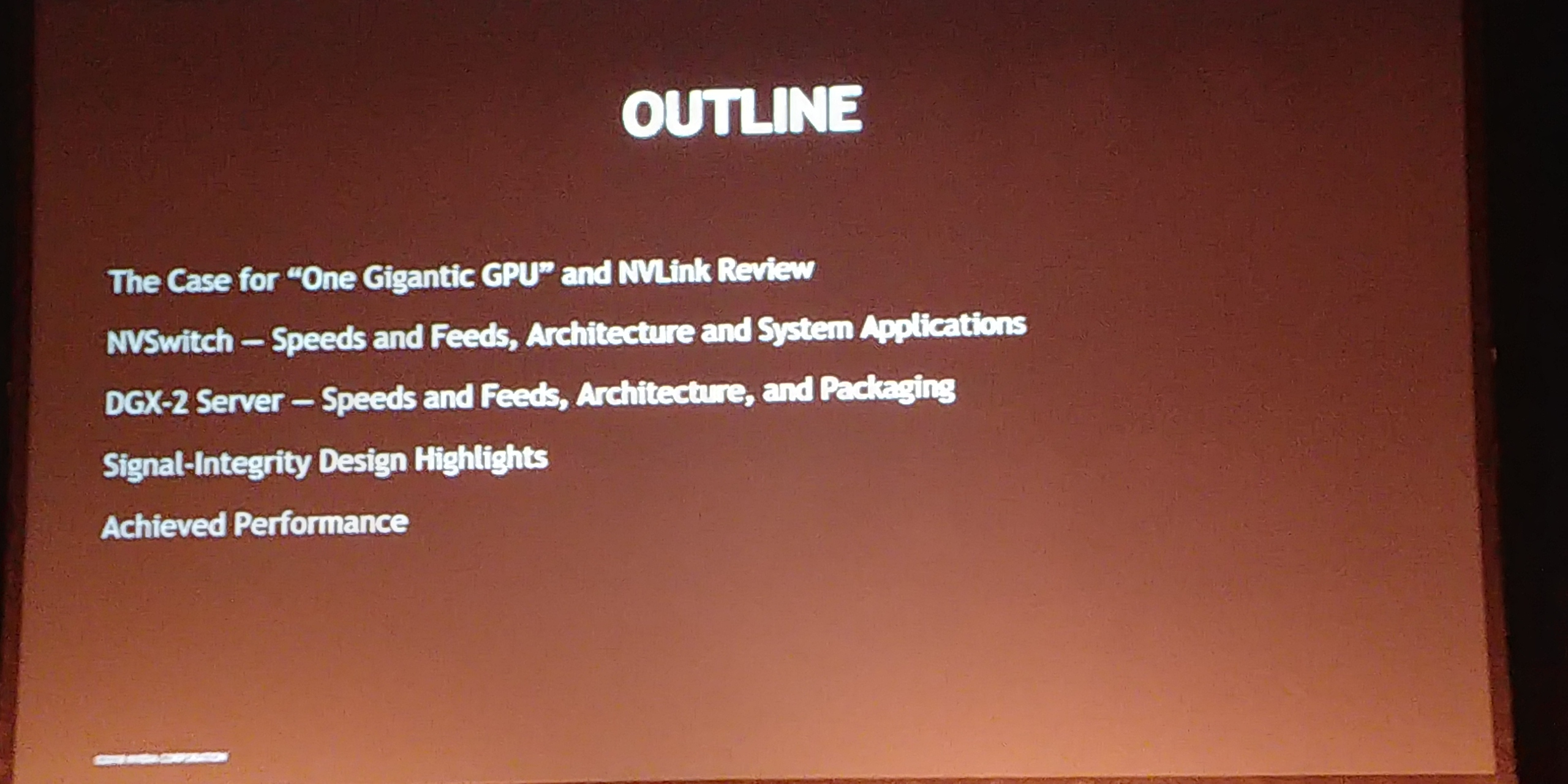
11:46AM EDT - The first talk on Day 2 of Hot Chips is from NVIDIA, going into more detail about how the NVSwitch works with a lot more detail than from previous talks. Also its implementation within DGX-2 is explored.
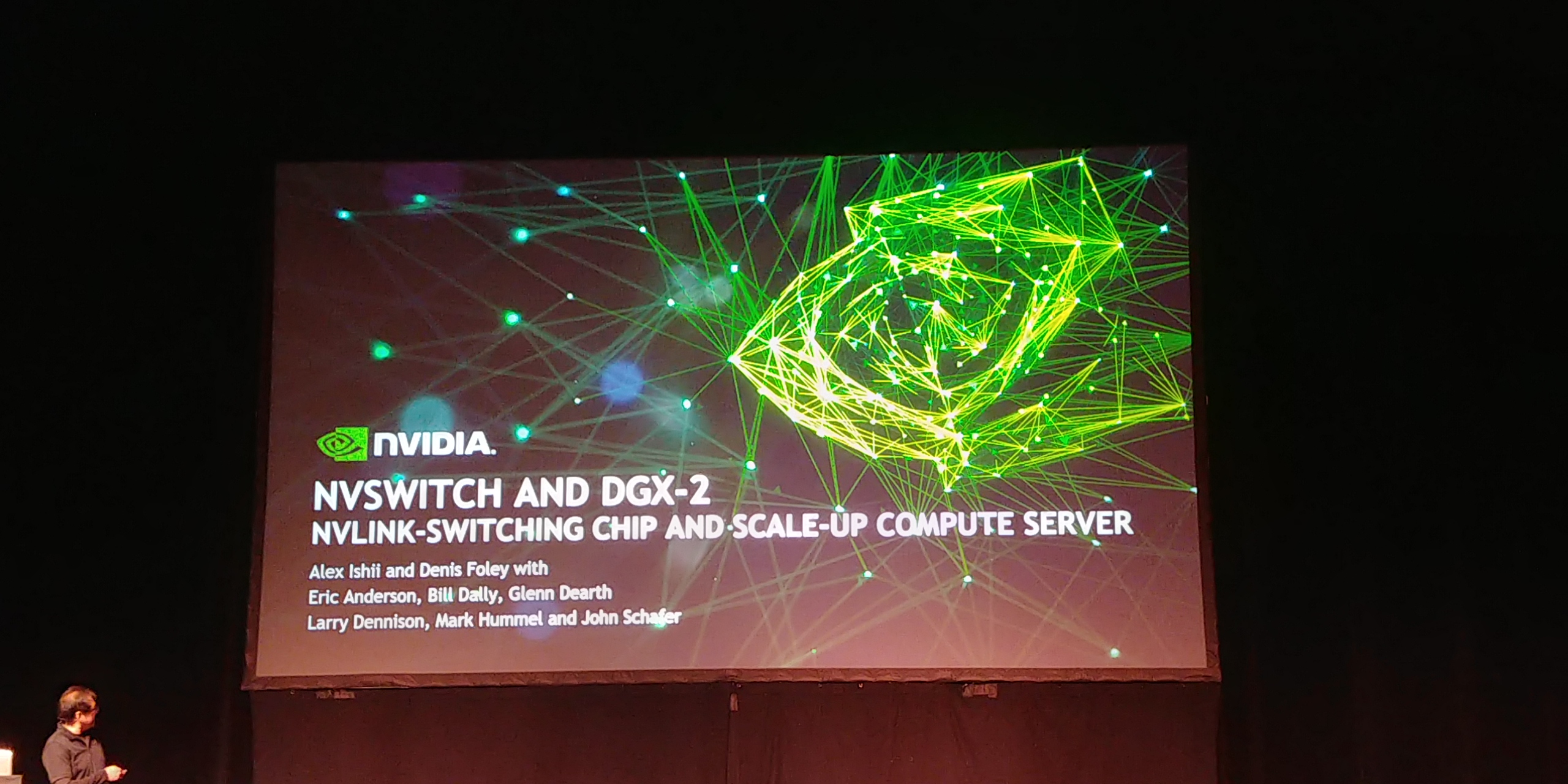
11:47AM EDT - NVSwitch and DGX-2 was originally a research program
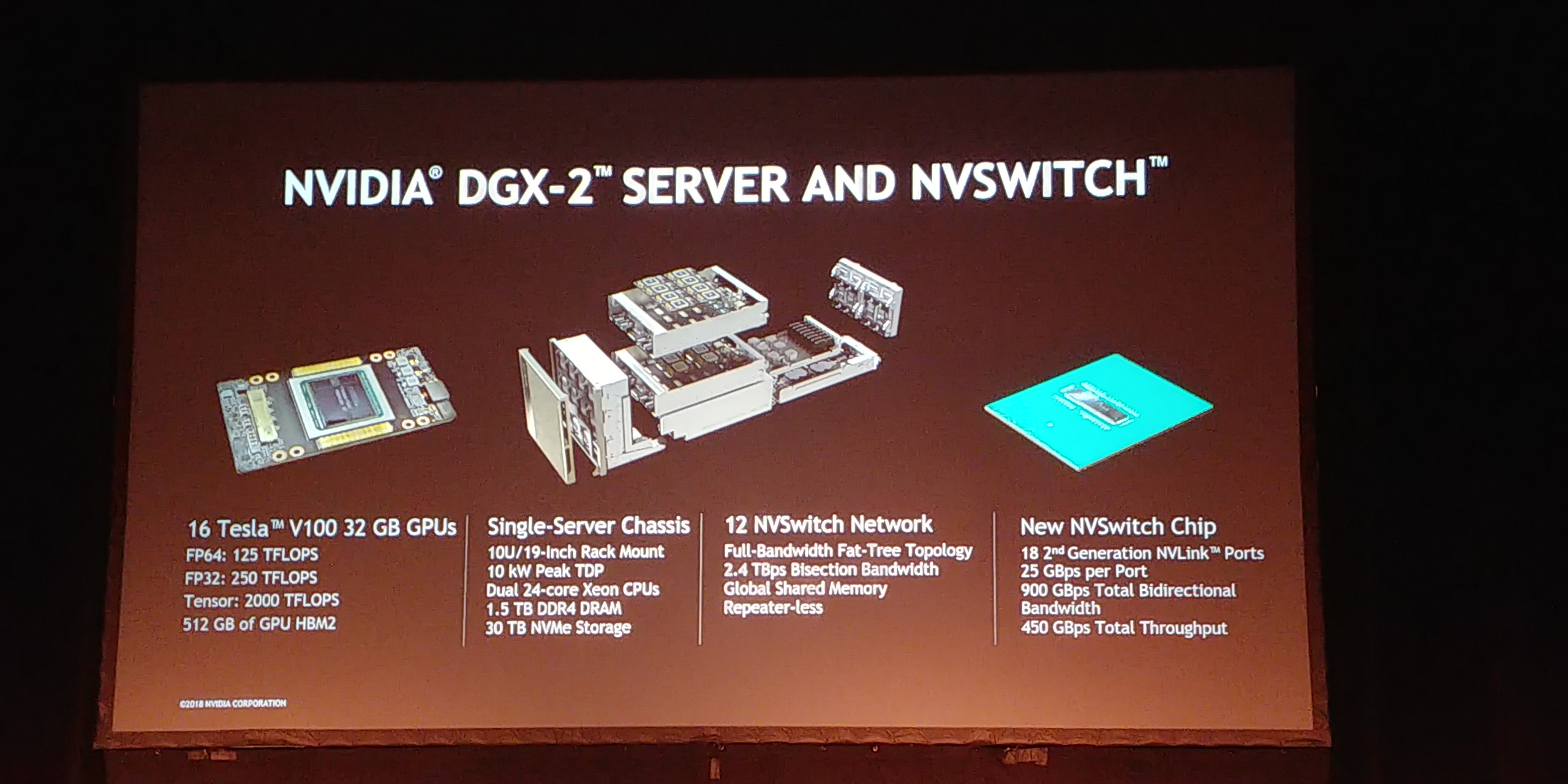
11:47AM EDT - DGX-2 has 16 V100s, 512GB of HBM2
11:47AM EDT - 10U chassis, 10kW Peak TDP
11:48AM EDT - Dual 24-core Xeons, 1.5TB DDR4
11:48AM EDT - 30 TB NVMe Storage
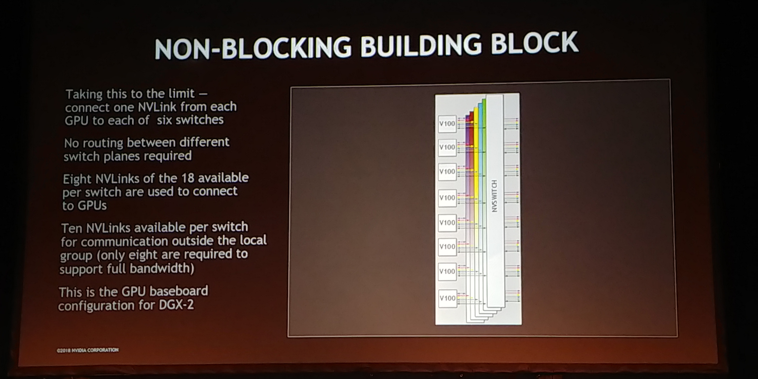
11:48AM EDT - Has 12 NVSwitches
11:48AM EDT - Full bandwidth fat-tree topology
11:48AM EDT - 2.4 TBps bisectional bandwidth
11:48AM EDT - Global shared memory
11:48AM EDT - repeater-less
11:48AM EDT - Every GPU works in the same address space
11:49AM EDT - 'One gigantic GPU'
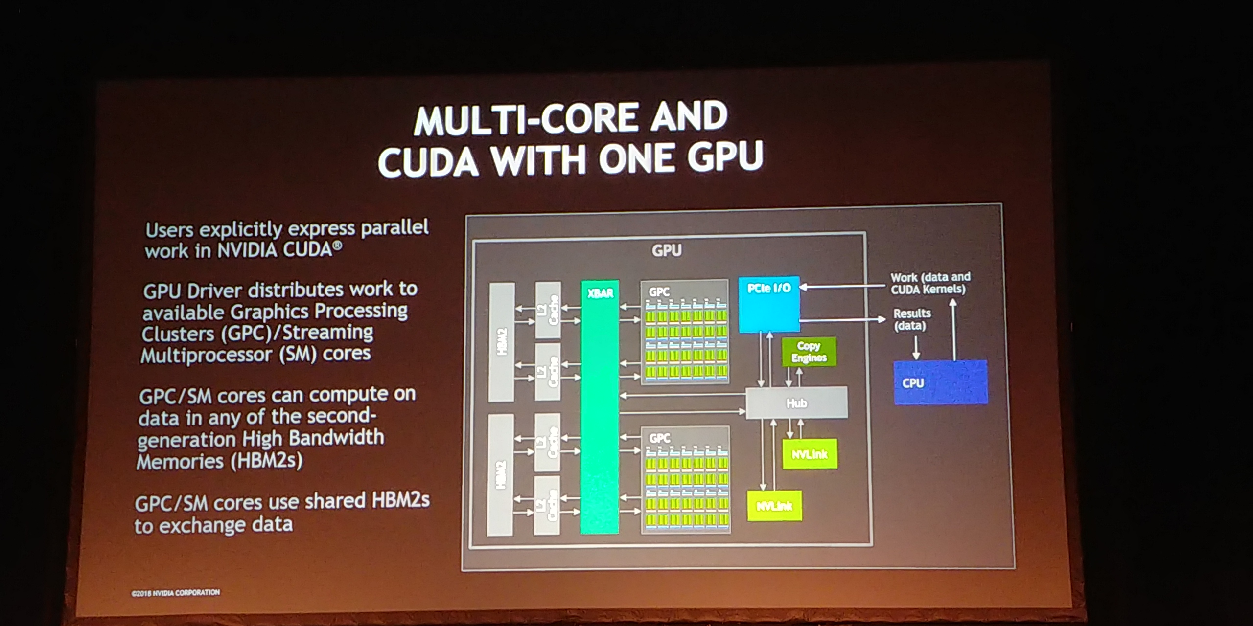
11:49AM EDT - With one GPU, the CPU tells the GPU what to run
11:50AM EDT - Explicit CUDA in parallel
11:50AM EDT - Crossbar implements shared data structure
11:51AM EDT - For two GPUs, accessing other GPU memory takes a long time. Limited by PCIe
11:51AM EDT - PCIe is the wild west
11:51AM EDT - NVLink gets around that
11:51AM EDT - NVLink has more BW, and multiple links
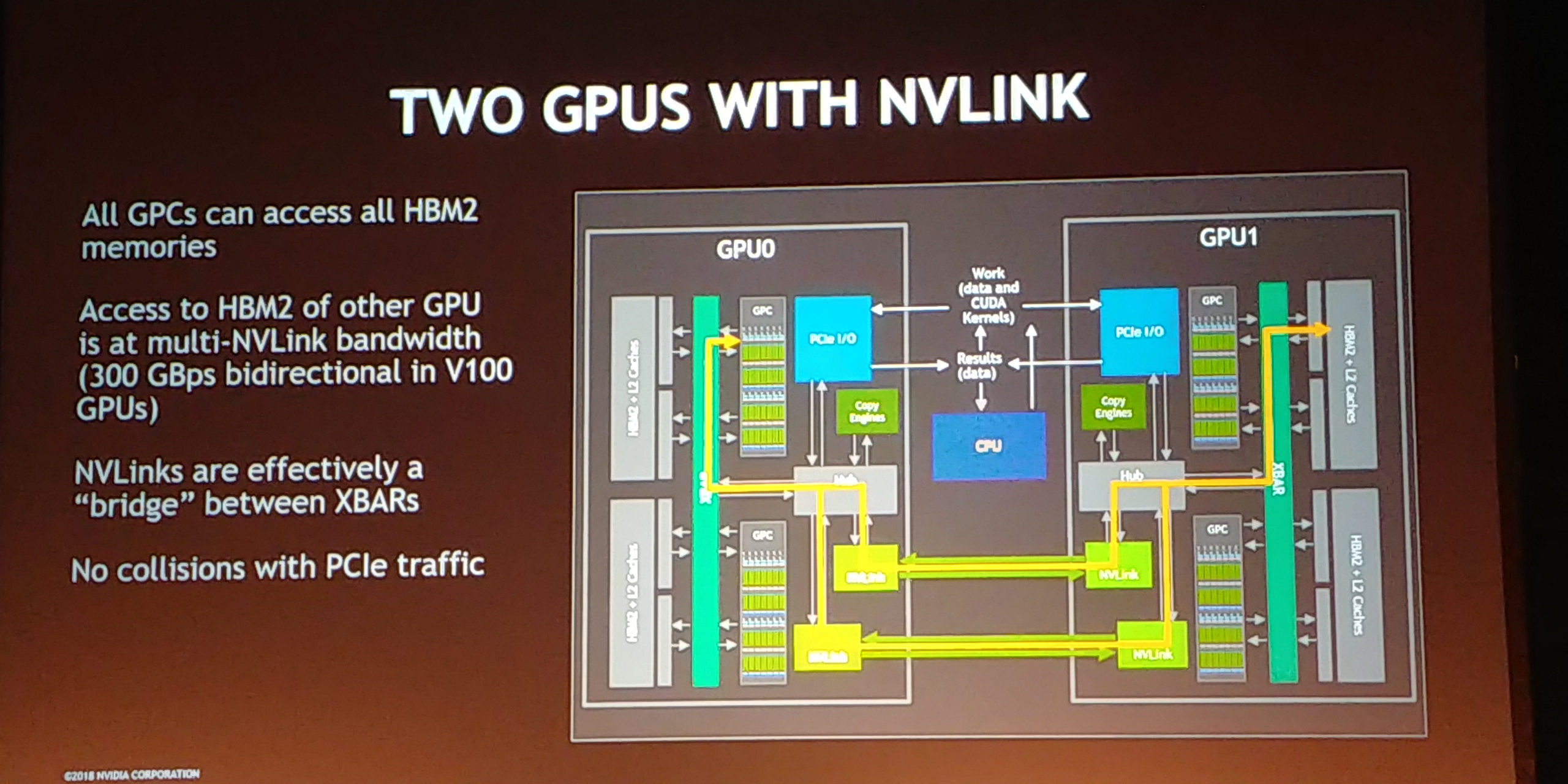
11:52AM EDT - With that much bandwdith, two GPUs looks like one GPU
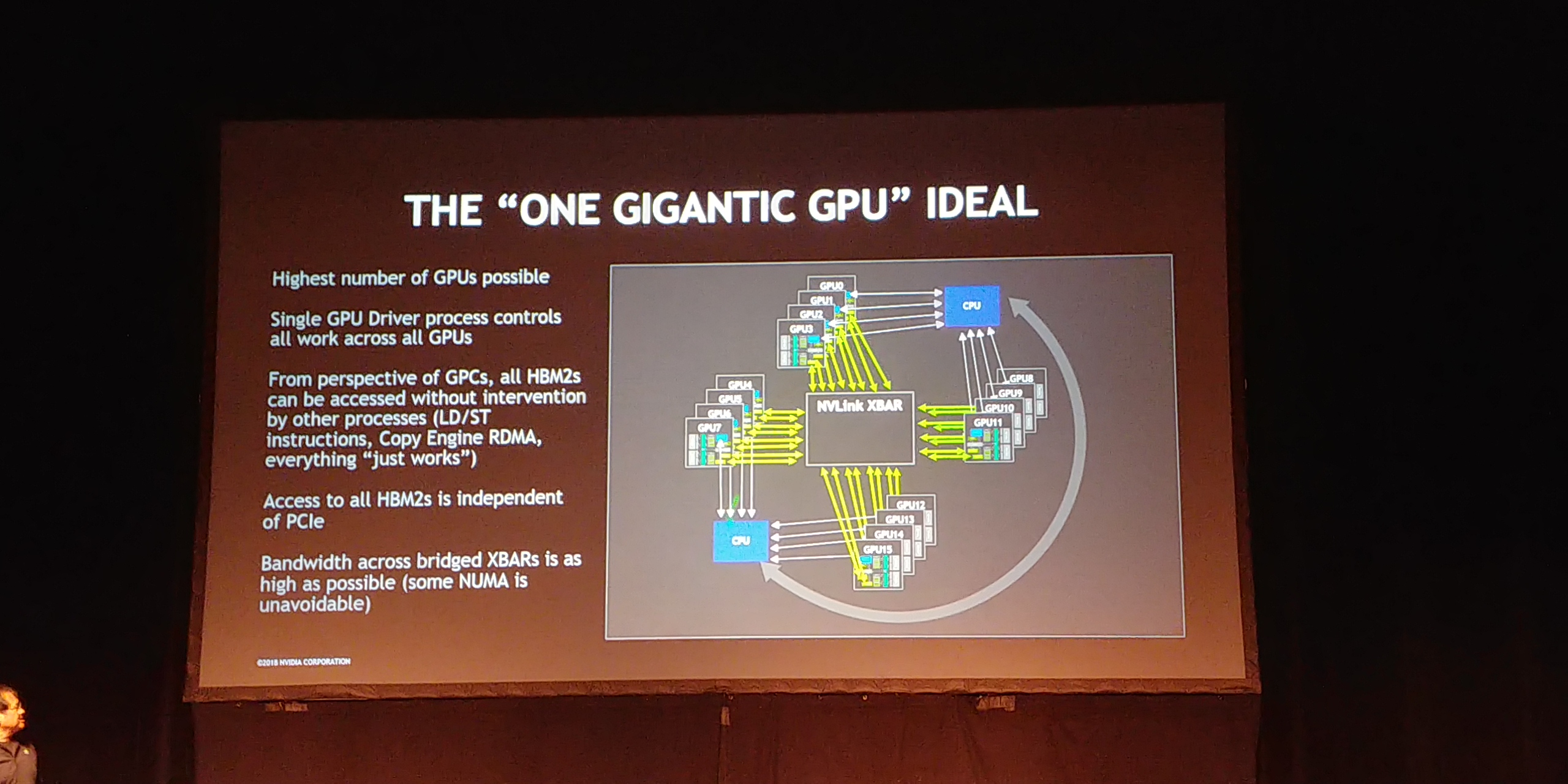
11:52AM EDT - Aim is to make as many GPUs as possible in a single system with a single GPU driver process
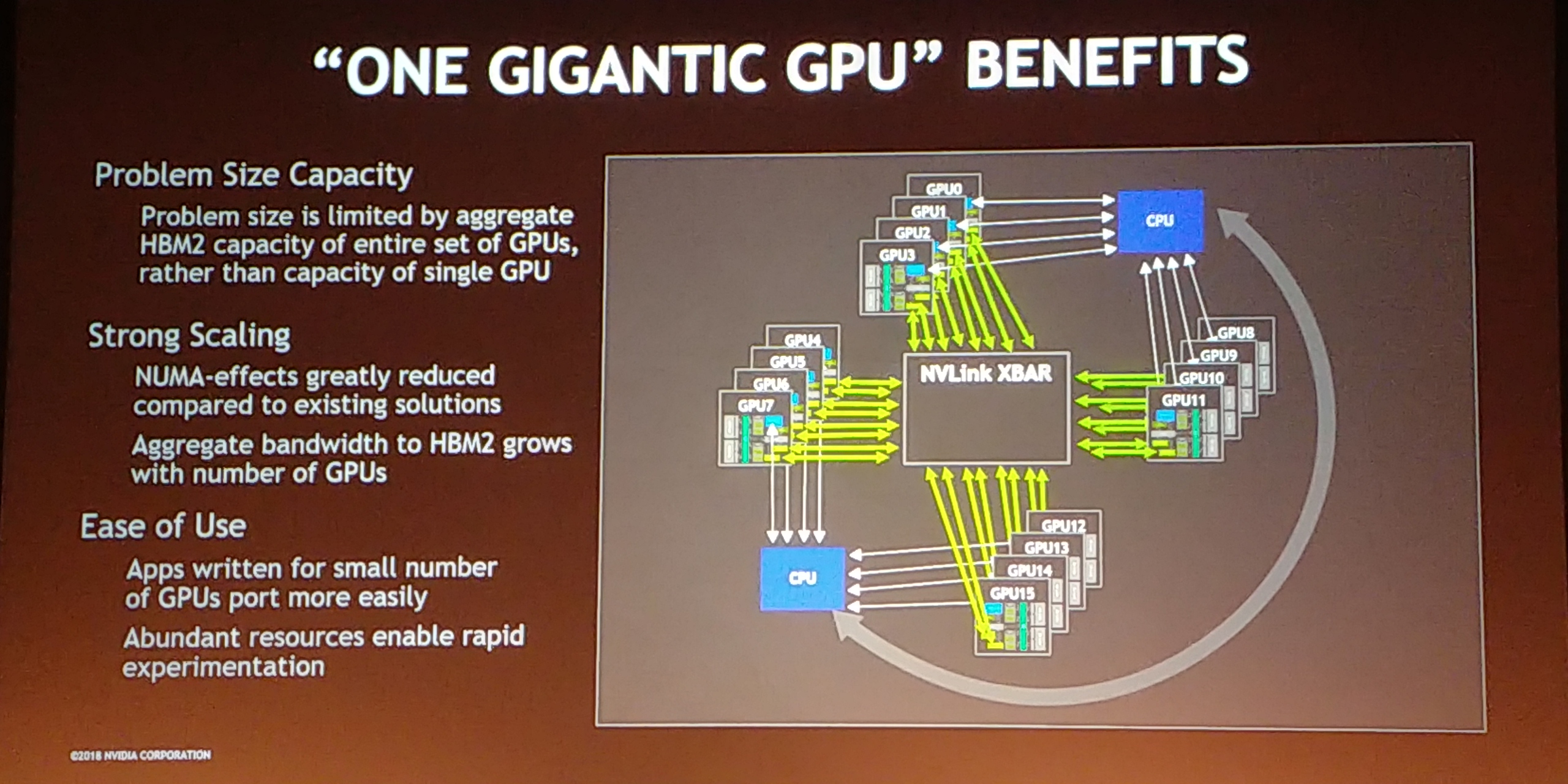
11:53AM EDT - Bypass memory limits as you can access all HBM on all GPUs from one GPU
11:53AM EDT - Also more HBM bandwidth
11:53AM EDT - Just need a decent crossbar for NVLink
11:53AM EDT - Strong scaling to reduce NUMA effects
11:54AM EDT - Programming model for small GPU software is ported easily
11:54AM EDT - more resources means rapid experimentation
11:54AM EDT - NVSwitch

11:54AM EDT - Has one PCIe port for management
11:55AM EDT - NVLink is really 51.5 GBps
11:55AM EDT - 106mm2 per die
11:55AM EDT - 2 billion transistors

11:55AM EDT - Not a normal networking switch
11:56AM EDT - Does not have a lot of networking features such as advanced QoS - it's designed just for GPUs and a known environment
11:56AM EDT - It's a bridging device
11:56AM EDT - Transforms are spoofing as if each GPU sees one other GPU
11:56AM EDT - that's where the magic is
11:56AM EDT - Was able to reuse a lot of design because it was 12 GGN
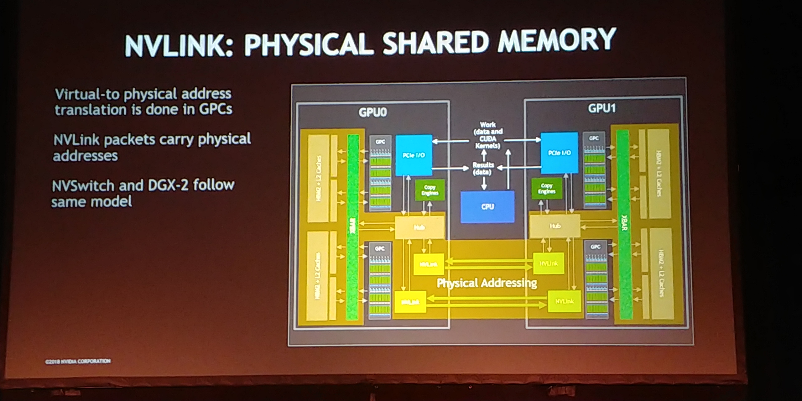
11:57AM EDT - NVLink packets carry physical addresses
11:57AM EDT - So NVSwitch also does the same
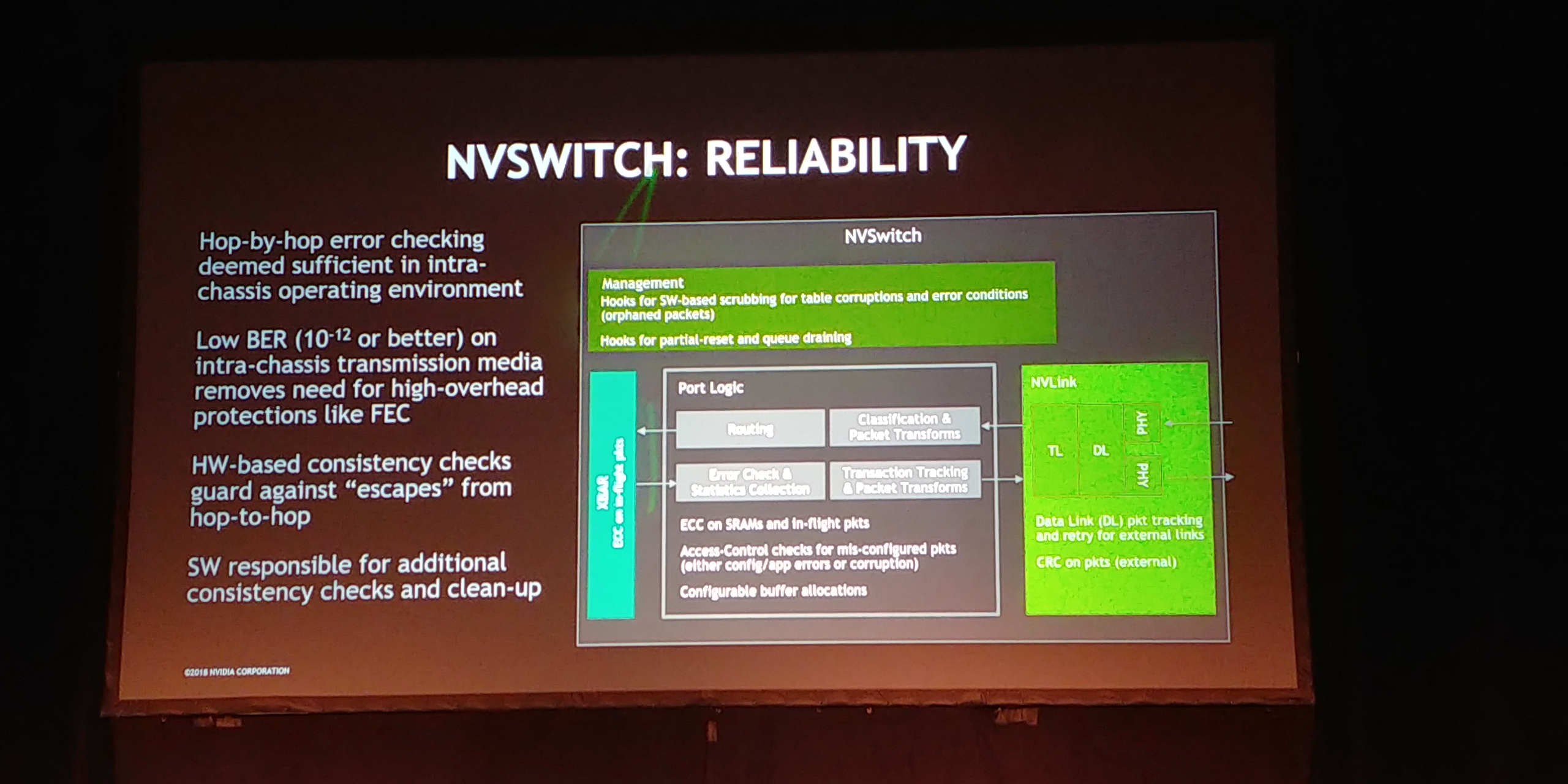
11:58AM EDT - Low error rate (10^-12)
11:58AM EDT - Good enough to just do CRC
11:58AM EDT - done on a hop-by-hop basis
11:58AM EDT - packet checking via software
11:58AM EDT - ECC on SRAMs and in-flight packets
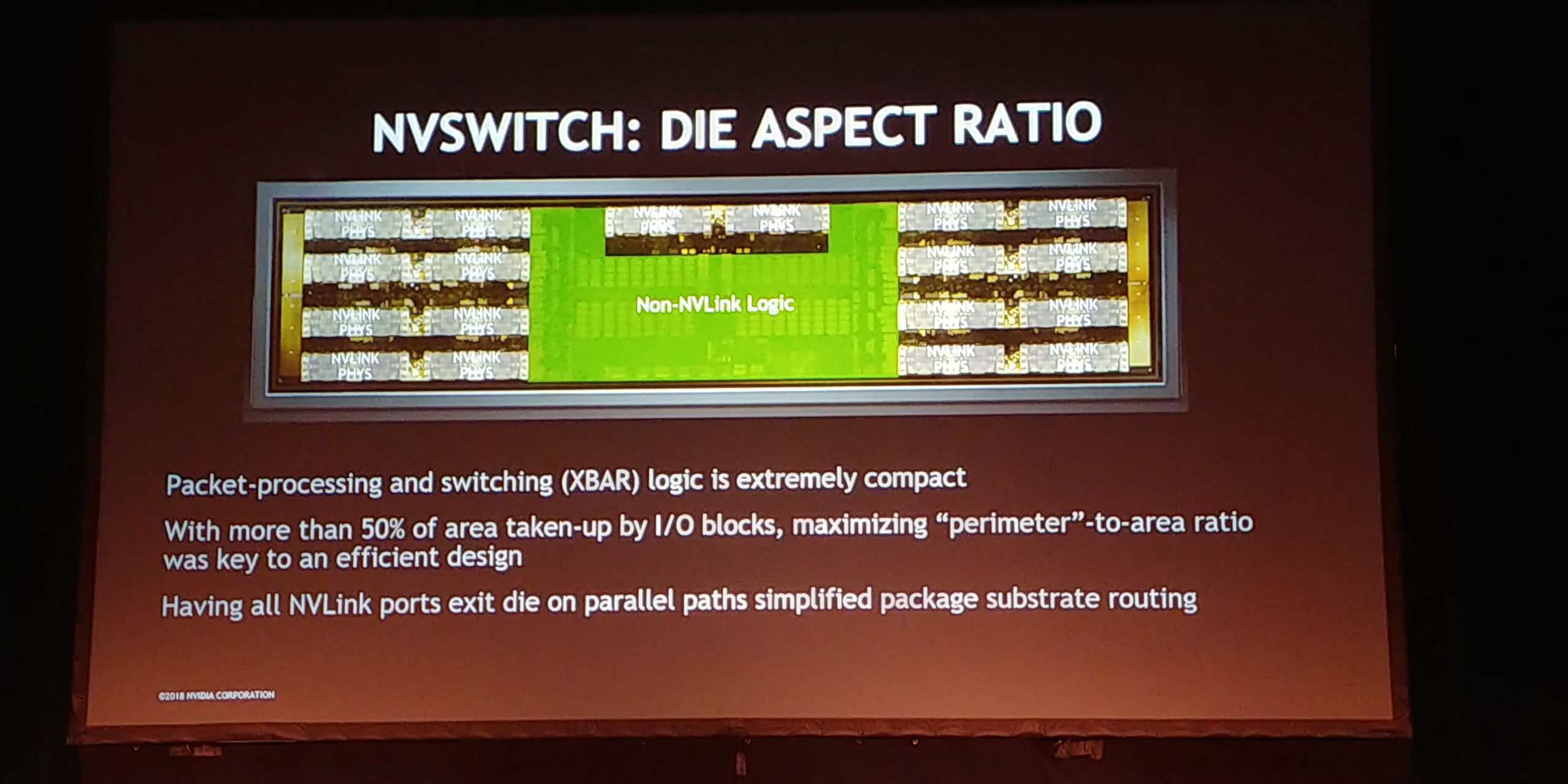
11:59AM EDT - Area for the logic is less than half the area
11:59AM EDT - Maximizing perimeter to area ratio was key to an efficieny design
11:59AM EDT - parallel paths simplify package substrate routing
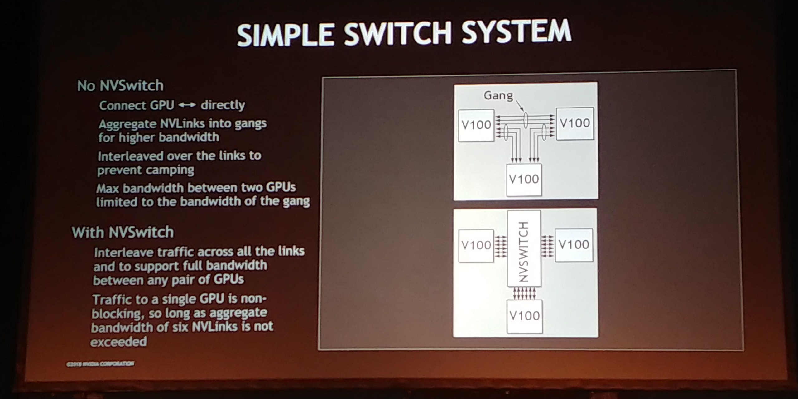
12:00PM EDT - Allows for full bandwidth to each GPU. Without NVSwitch, bandwidth would be 1/(n-1) x
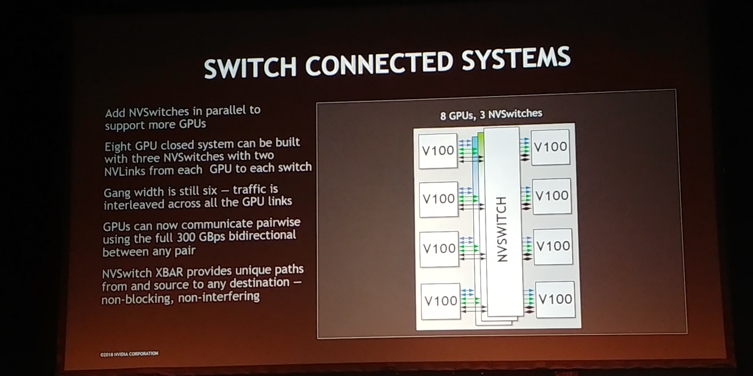
12:01PM EDT - Each GPU can talk to each other
12:01PM EDT - At the same time
12:01PM EDT - non-blocking

12:01PM EDT - Everything just works
12:02PM EDT - Could have used just 6 switches, but makes manufacturing and routing easier

12:02PM EDT - List of specs
12:03PM EDT - All air cooled
12:03PM EDT - 1000 CFM air flow
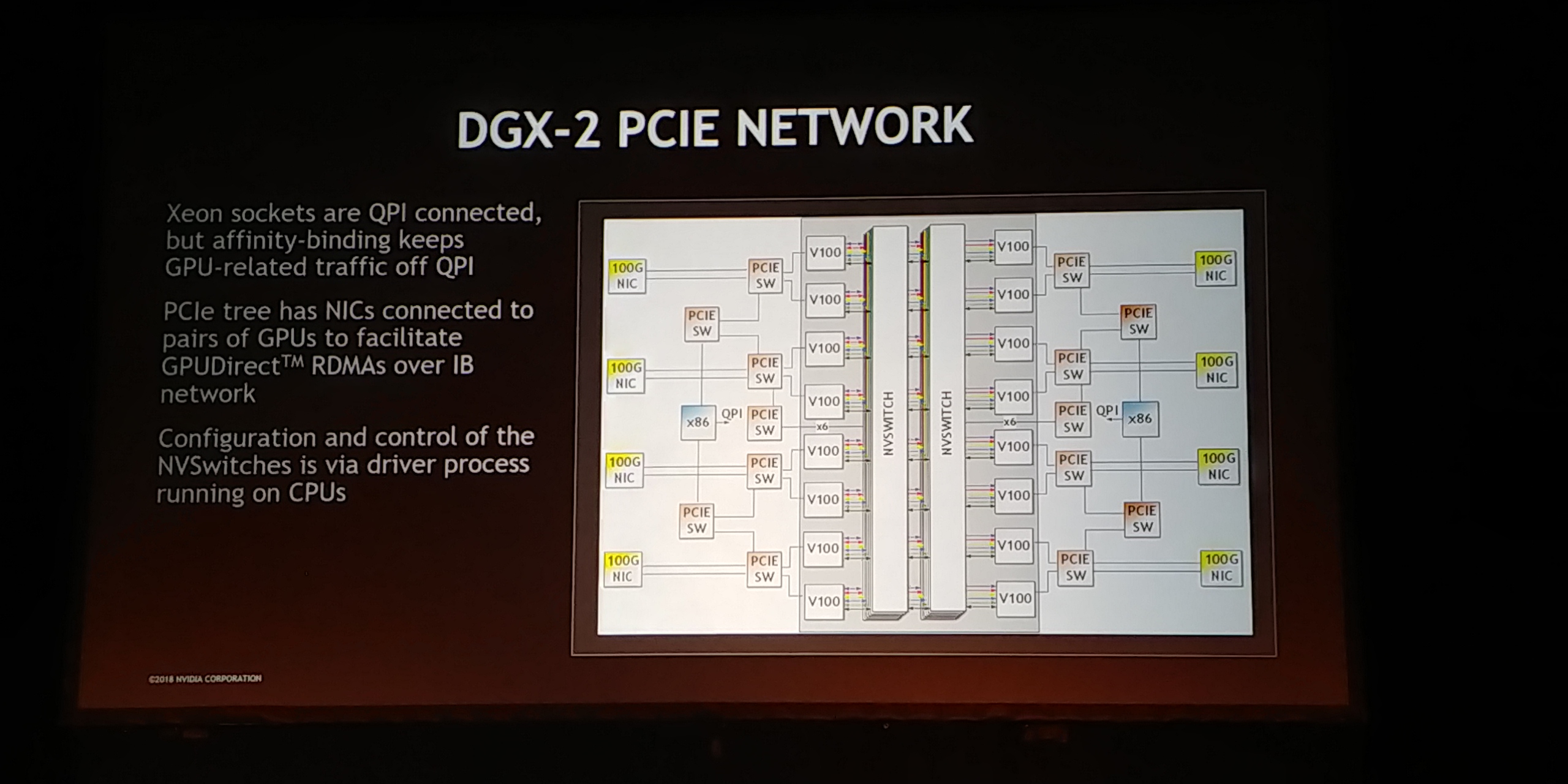
12:03PM EDT - PCIe switch network to deal with infiniband and GPUs
12:03PM EDT - Each NIC has a clean path to two GPUs for RDMA
12:04PM EDT - PCIe switch for control to NVSwitches
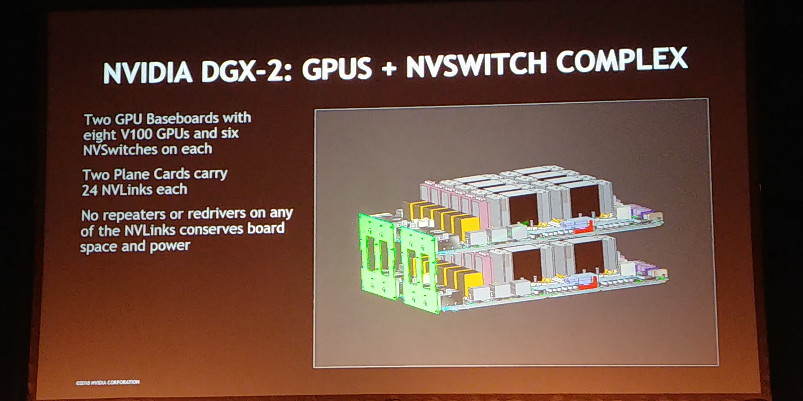
12:04PM EDT - Two GPU baseboards connected with a plane card with no repeaters or buffers
12:04PM EDT - 144 NVLinks total
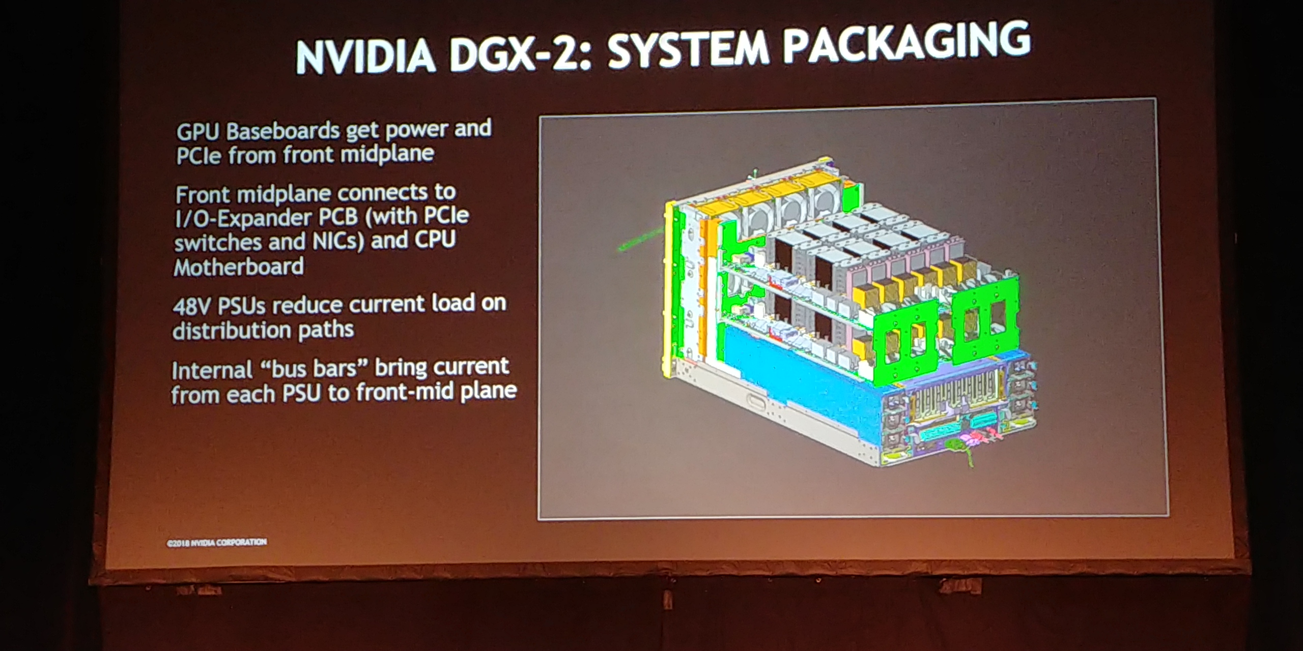
12:05PM EDT - 48V power distribution
12:05PM EDT - Copper bus bars to get current up to the planes
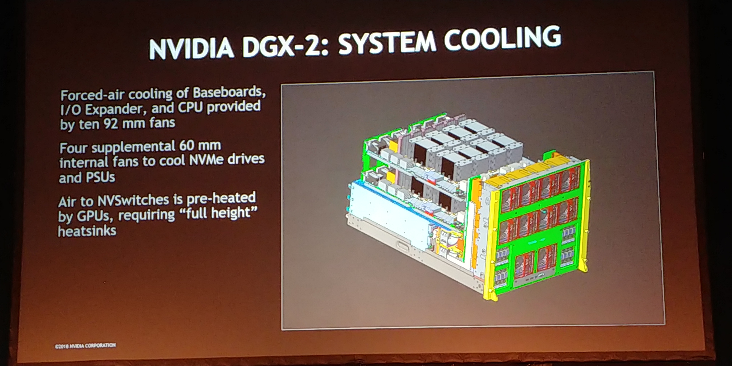
12:06PM EDT - ten 92mm fans
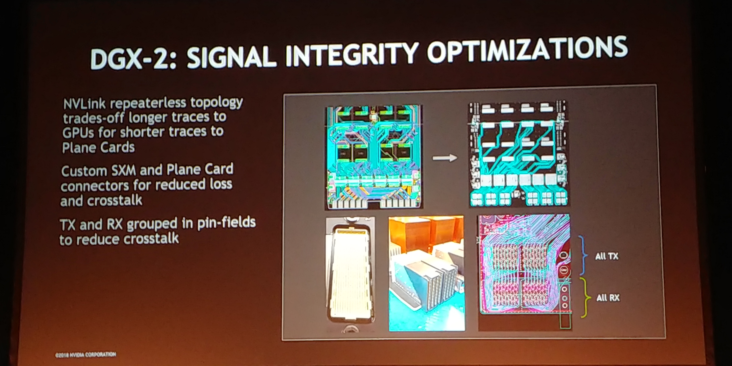
12:06PM EDT - Custom SXC and plane card connectors
12:07PM EDT - Went from quad GPU talking to triplet switches, but did 8 to 6 with longer traces to enable low bit error rates
12:07PM EDT - makes it simpler with less tracing talk over
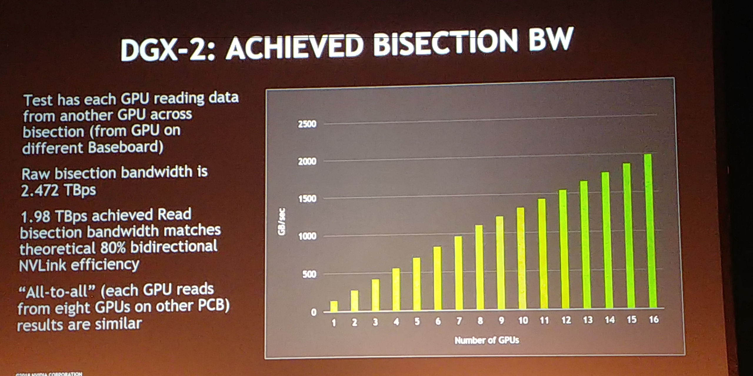
12:08PM EDT - Scales in bandwidth up to 2 TBps
12:08PM EDT - near true bisectional bandwidth
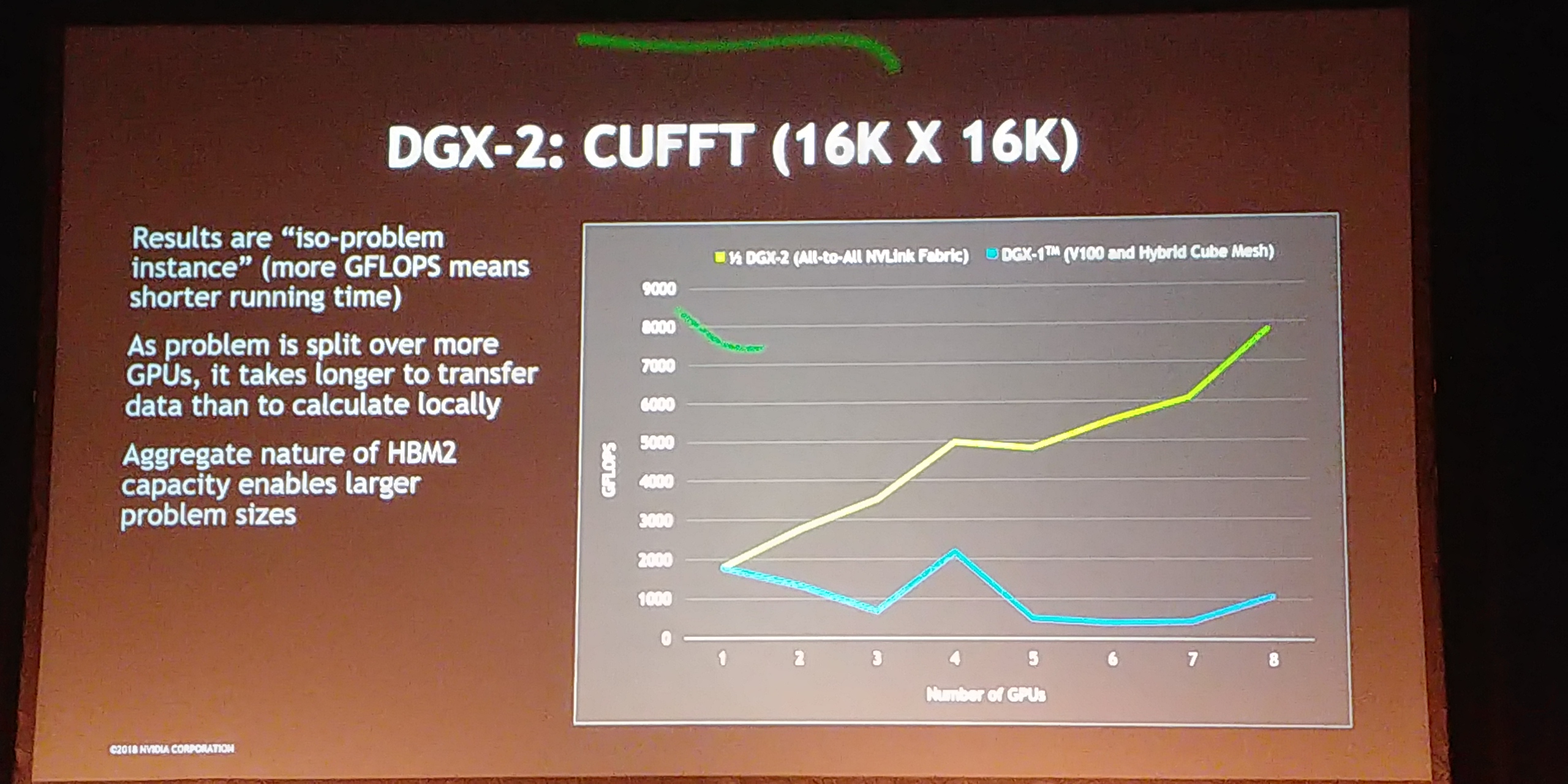
12:08PM EDT - FFT compute scales with GPUs
12:09PM EDT - This is a test with lots of cross-memory bandwidth requirements
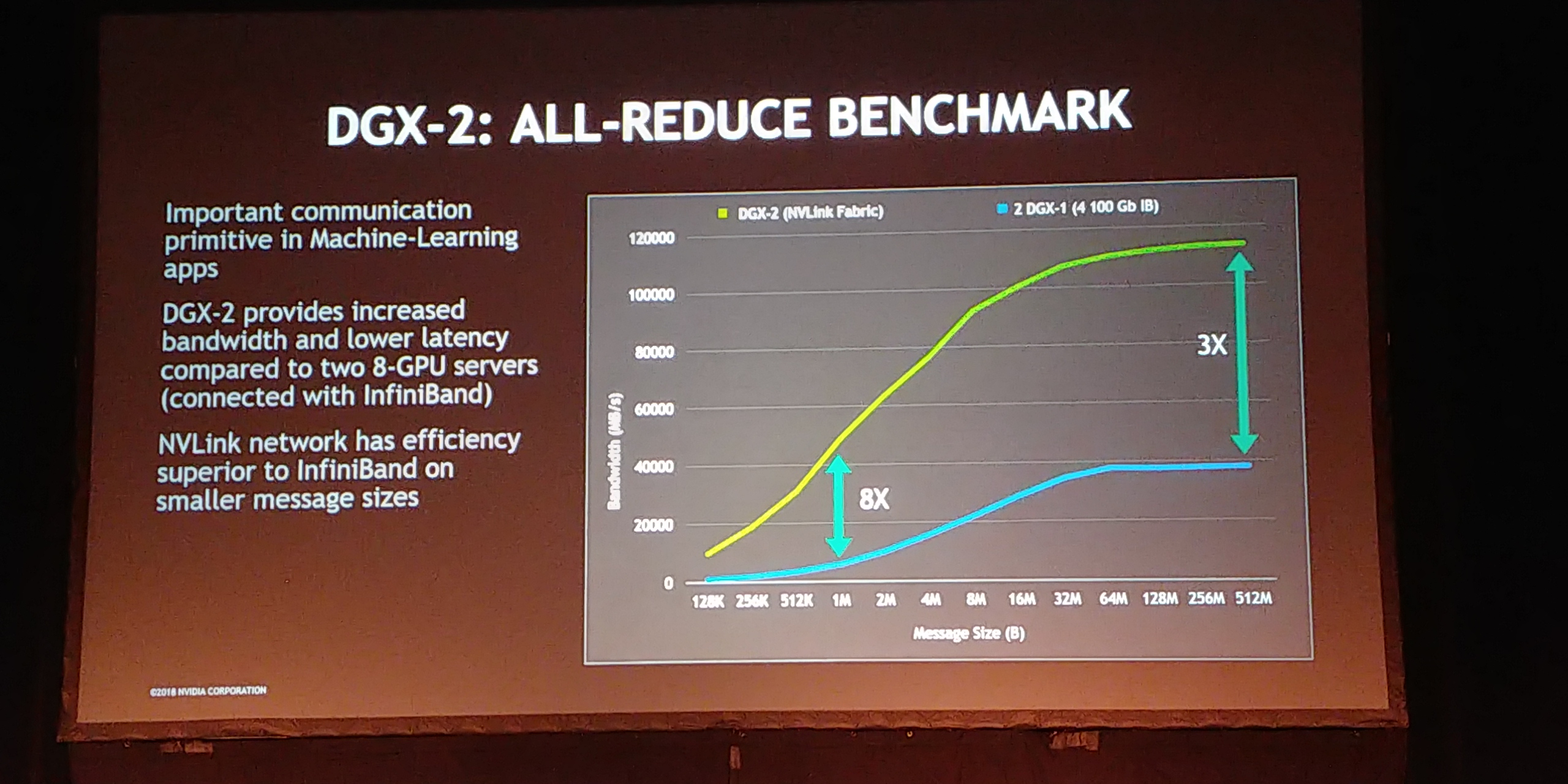
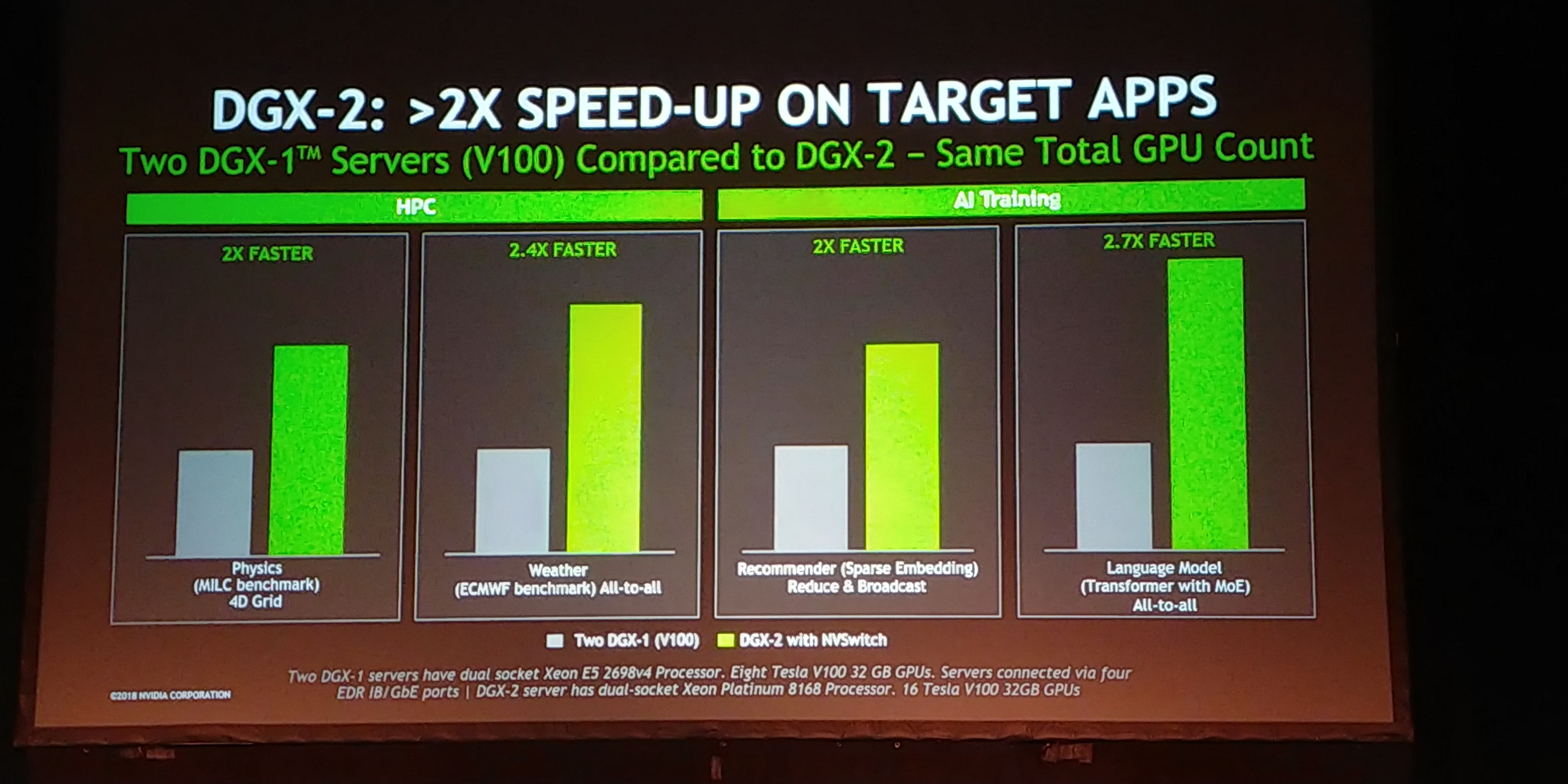
12:09PM EDT - For all-reduce, 3-8x bandwidth increase over two DGX-1 machines
12:10PM EDT - At small message size, also low latency leads to 8x
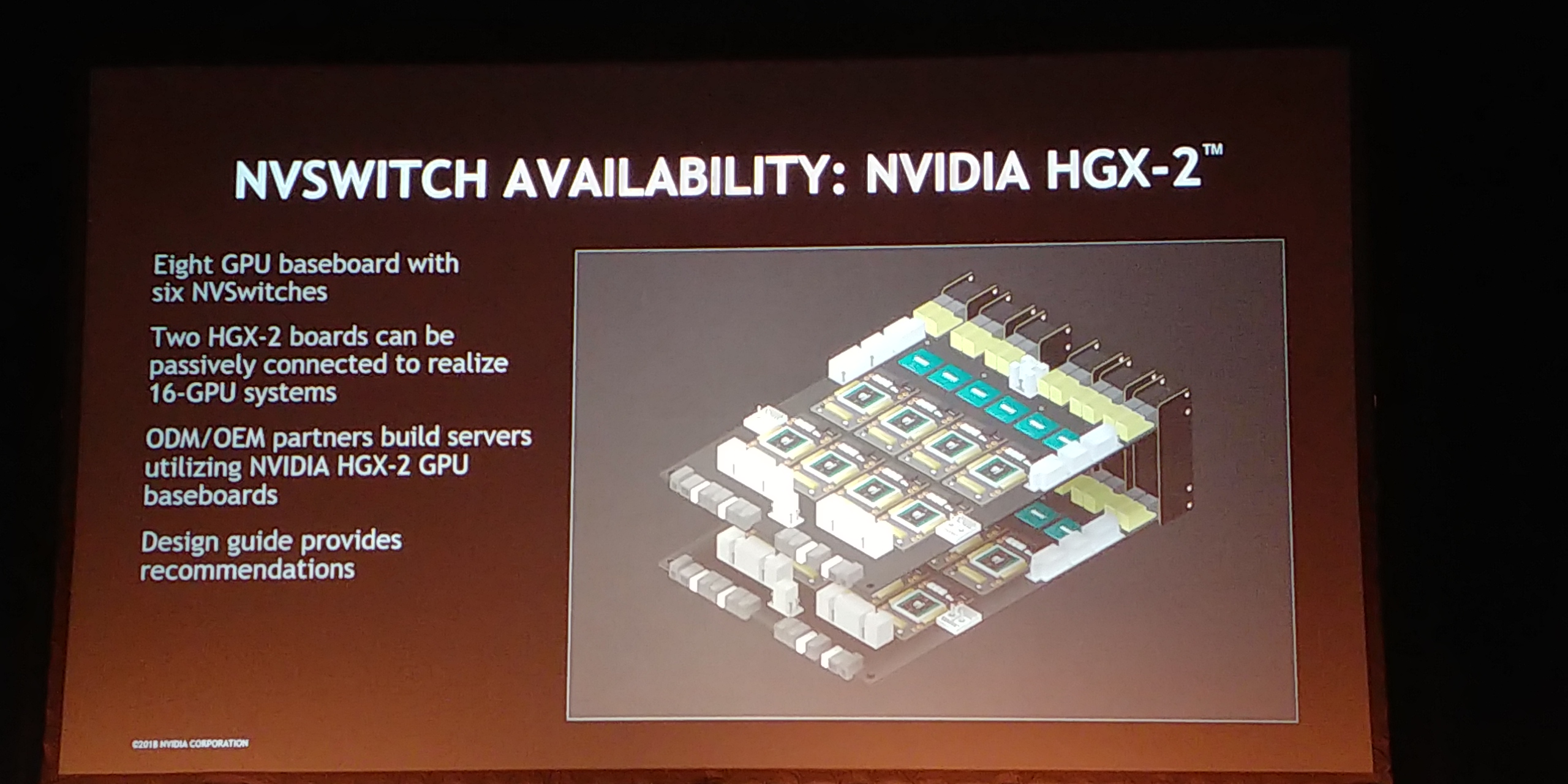
12:10PM EDT - Can't buy the switches, but can buy the DGX-2
12:11PM EDT - Can buy HGX-2 and custom a lot of the rest of the system
12:11PM EDT - Q and A time
12:12PM EDT - Q: Power of ASIC? A: I've been asked not to say. Lower than you would expect - our PHYs are more efficient than average because we're in 12nm. Calculate from the area!
12:13PM EDT - Q: Why does bisectional bandwidth drop off after 8 GPUs? A: These are read operations. In order to read, it requires a request - the request has to across the board-to-board bisection. Those requests start eating into the bandwidth, but it's very linear
12:13PM EDT - That's all for now. Next Live Blog is in 30 minutes, about NRAM.


2 Comments
View All Comments
skavi - Tuesday, August 21, 2018 - link
Does NVLink really take up 106mm^2 per die? How does that compare to whatever area a PCIe connection took up? Is it the same in Turing?eastcoast_pete - Thursday, August 23, 2018 - link
My favorite line: "PCIe is the wild west" . The question is now who will be the new sheriff in town? NVLink?