Samsung’s Multi-Billion Fab in Pyeongtaek Starts Production of 64-Layer V-NAND
by Anton Shilov on July 6, 2017 11:30 AM EST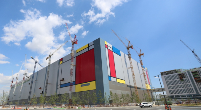
Samsung on Tuesday announced that it had started mass production of 64-layer V-NAND memory in its newly build fab in Pyeongtaek, South Korea, and the first batch had already been shipped to one of the company’s customers. The new fab was intended to focus on DRAM manufacturing, but in the light of NAND flash shortage the company adjusted its plans at some point and now the plant produces V-NAND.
Samsung’s semiconductor manufacturing facility in Pyeongtaek will be the largest and one of the most expensive fabs in the world once it ramps up its production to full capacity. Samsung announced plans to build it in October, 2014, and then started construction in April, 2015. Initially, Samsung announced plans to invest ₩15.6 trillion (around $13.5 billion at the current exchange rate) in the facility, but over the past couple of years, it announced further expansion plans for the fab. As a result, investments in the Pyeongtaek facility will total ₩30 trillion ($26.1 billion) by 2021, making the complex the most expensive semiconductor manufacturing facility ever.
According to some reports, Samsung initially planned to produce DRAM in its new fab, but given its size and scale, it was doubtful that the plant would be used only for DRAM. As it appears, Samsung decided to produce fourth-generation 3D V-NAND flash memory in its Pyeongtaek facility first, possibly because there is growing demand for NAND by Samsung’s own divisions, including Samsung Mobile. It remains to be seen when the fab in Pyeongtaek starts to manufacture DRAM ICs, which are also in short supply nowadays. Keep in mind that 3D NAND and DRAM components are produced using completely different process technologies and the former requires some additional equipment. Therefore, Samsung and other memory makers cannot switch from NAND to DRAM and vice versa without some level of equipment adjustment and reconfiguration of fab space.
At present, Samsung does not talk about the number of wafer starts at the Pyeongtaek fab because it is not operating at full capacity. That said, the plant is not going to have a substantial impact on global NAND supply in the coming weeks or months. Once fully ramped several quarters down the road, the Pyeongtaek facility will have a significant impact on both NAND and DRAM industries, as it will increase the output of both types of memory (assuming that it will be used for DRAM in the coming quarters).
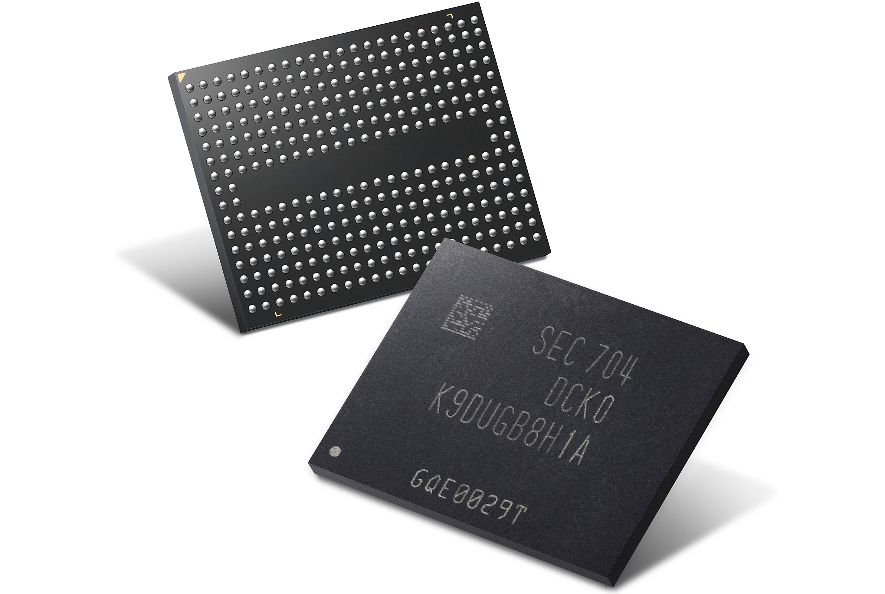
Samsung does not disclose what kind of flash memory chips it produces in terms of capacity and performance, but says that they rely on its 64-layer V-NAND design. So far, the company officially has announced only two 64-layer V-NAND ICs. First is the 512 Gb 3D TLC NAND chip with an 800 MT/s interface data rate that the company demonstrated at the Flash Memory Summit 2016. Second, the 256 Gb 3D TLC NAND IC with a 1000 MT/s interface data rate, the company launched earlier this year and began to produce in high volume in June (presumably at another facility).
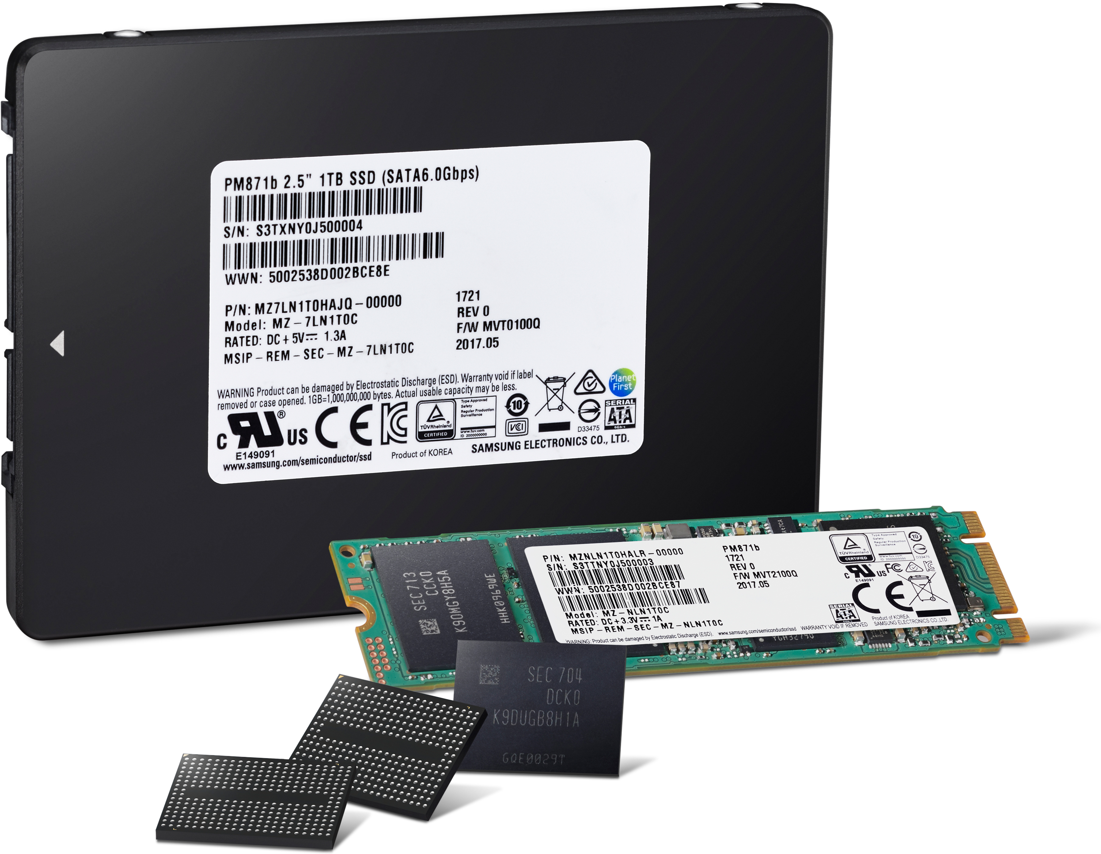
Manufacturing of 64-layer 256 Gb chips in at least two facilities indicates that Samsung is ramping up volume production of its fourth-generation V-NAND chips and therefore it is logical to expect new products based on such ICs (e.g., SSDs, memory cards, etc.) to hit the market in the coming months. Among the more interesting products will be higher-end SSDs based on 256 Gb V-NAND chips featuring a faster interface, but it remains to be seen what kind of real-world performance advantages they are going to bring given the bandwidth limitations of PCIe 3.0 x4 bus (used for NVMe M.2 drives), or for smaller capacities. So far, Samsung has only introduced the OEM-oriented PM871b SATA SSDs in 2.5" and M.2 form-factors based on its fourth-gen V-NAND memory.
Related Reading
- Samsung at Flash Memory Summit: 64-layer V-NAND, Bigger SSDs, Z-SSD
- Samsung Announces 960 PRO And 960 EVO M.2 PCIe SSDs (Updated)
- The Samsung 960 Pro (2TB) SSD Review
- The Samsung 960 EVO (1TB) Review
- SK Hynix Launches 72-Layer 256 Gb 3D TLC NAND with Increased Performance
- Western Digital Announce BiCS4 3D NAND: 96 Layers, TLC & QLC, Up to 1 Tb per Chip
- Toshiba's 768Gb 3D QLC NAND Flash Memory: Matching TLC at 1000 P/E Cycles?
Source: Samsung


16 Comments
View All Comments
melgross - Thursday, July 6, 2017 - link
Aren’t all fabs these days “multibillion”? I’m not impressed by the number, it’s expected.Space Jam - Thursday, July 6, 2017 - link
Even by fab standards its pricey.JCB994 - Thursday, July 6, 2017 - link
Cost is not so much the building but in the equipment. When Photo tools go for >$100 million, costs add up quickly.Samus - Thursday, July 6, 2017 - link
20 billion is about half of global foundaries net worth. That's pretty significant because this is just ONE fab compared to a conglomerate of multiple high tech fabs.name99 - Thursday, July 6, 2017 - link
There are lots of fabs building lots of things...A fab for lowish-end optical components or for some MEMS might run for under $10 million, especially if you are willing to outsource some steps of the manufacturing that are best done by alternative sorts of equipment (eg outsourcing optical coating or the MEMS assembly).
Samus - Thursday, July 6, 2017 - link
GloFo has two of the most advanced fabs in the world (and 10 fabs total) with Fab 1 in Dresden Germany and Fab 8 in Saratoga County New York both being 300mm production...Fab 1 has among the highest production capacity of any single fab in the world and Fab 8 is cutting edge 12nm finfet running at maximum production capacity with class leading yields. GloFo yields have been marginally, but consistently, better than TSMC's during the last 3 process node shrinks. TSMC is also heavily dependent on a single customer, NVidia, for over half of their business. GloFo produces chips for Qualcomm, STMicro, Broadcom, AMD, and IBM.GloFo also tapped out 7nm samples for customers this year with production beginning next year at 300mm, stating they could actually do it now but insist on tighter yields and cite they have plenty of time to still beat competitors to market because they jumped 10nm unlike everyone else.
But most importantly is the fact anybody can place orders at GloFo. They even have teams dedicated to helping you design ASICs. Samsung...doesn't really FAB for other people.
Tams80 - Friday, July 7, 2017 - link
Samsung, at the moment at least, does manage to fulfil depend internally for the most part, with some big customers taking up the rest. With this fab, maybe they will have some to spare. That doesn't take into account them being South Korean though, which might make it harder for smaller companies to get help from them.As for GlobalFoundries, while they are doing well now, let's not forget their 14nm FinFET design failed, and they had to license Samsung's design. Luck changes quickly in this industry.
vladx - Sunday, July 9, 2017 - link
And yet most if not all of TSMC-based products trounce the GloFo-based ones.Eric Klien - Wednesday, July 12, 2017 - link
"TSMC is also heavily dependent on a single customer, NVidia, for over half of their business."This isn't even close to being correct so everything else you said is likely wrong as well. Nvidia is about 5% of their business (although getting larger over time). Financial Times said, "In 2016, TSMC’s top two customers were Apple and Qualcomm, which contributed 17 per cent and 11 per cent, respectively, to its revenue." at https://www.ft.com/content/80feb372-3177-11e7-9555...
lilmoe - Thursday, July 6, 2017 - link
Lower prices please.