Intel Executive Posts Thunderbolt 5 Photo then Deletes It: 80 Gbps and PAM-3
by Dr. Ian Cutress on August 1, 2021 1:29 PM EST
An executive visiting various research divisions across the globe isn’t necessarily new, but with a focus on social media driving named individuals at each company to keep their followers sitting on the edge of their seats means that we get a lot more insights into how these companies operate. The downside of posting to social media is when certain images exposing unreleased information are not vetted by PR or legal, and we get a glimpse into the next generation of technology. That is what happened today.
Day 1 with the @intel Israel team in the books. Great views…incredible opp to see @GetThunderbolt innovation …a validation lab tour and time with the team…can’t wait to see what tomorrow brings! pic.twitter.com/GKOddA6TNi
— Gregory M Bryant (@gregorymbryant) August 1, 2021
EVP and GM of Intel’s Client Computing Group, Gregory Bryant, is this week spending some time at Intel’s Israel R&D facilities in his first overseas Intel trip in of 2021. An early post on Sunday morning, showcasing Bryant’s trip to the gym to overcome jetlag, was followed by another later in the day with Bryant being shown the offices and the research. The post contained four photos, but was rapidly deleted and replaced by a photo with three (in the tweet above). The photo removed showcases some new information about next-generation Thunderbolt technology.
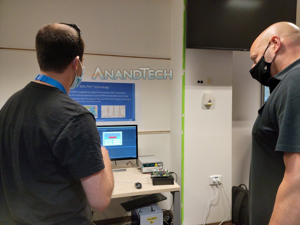
In this image we can see a poster on the wall showcasing ‘80G PHY Technology’, which means that Intel is working on a physical layer (PHY) for 80 Gbps connections. Off the bat this is double the bandwidth of Thunderbolt 4, which runs at 40 Gbps.
The second line confirms that this is ‘USB 80G is targeted to support the existing USB-C ecosystem’, which follows along that Intel is aiming to maintain the USB-C connector but double the effective bandwidth.
The third line is actually where it gets technically interesting. ‘The PHY will be based on novel PAM-3 modulation technology’. This is talking about how the 0 and 1s are transmitted – traditionally we talk about NRZ encoding, which just allows for a 0 or a 1 to be transmitted, or a single bit. The natural progression is a scheme allowing two bits to be transferred, and this is called PAM-4 (Pulse Amplitude Modulation), with the 4 being the demarcation for how many different variants two bits could be seen (either as 00, 01, 10, or 11). PAM-4, at the same frequency, thus has 2x the bandwidth of an NRZ connection.
So what on earth in PAM-3?
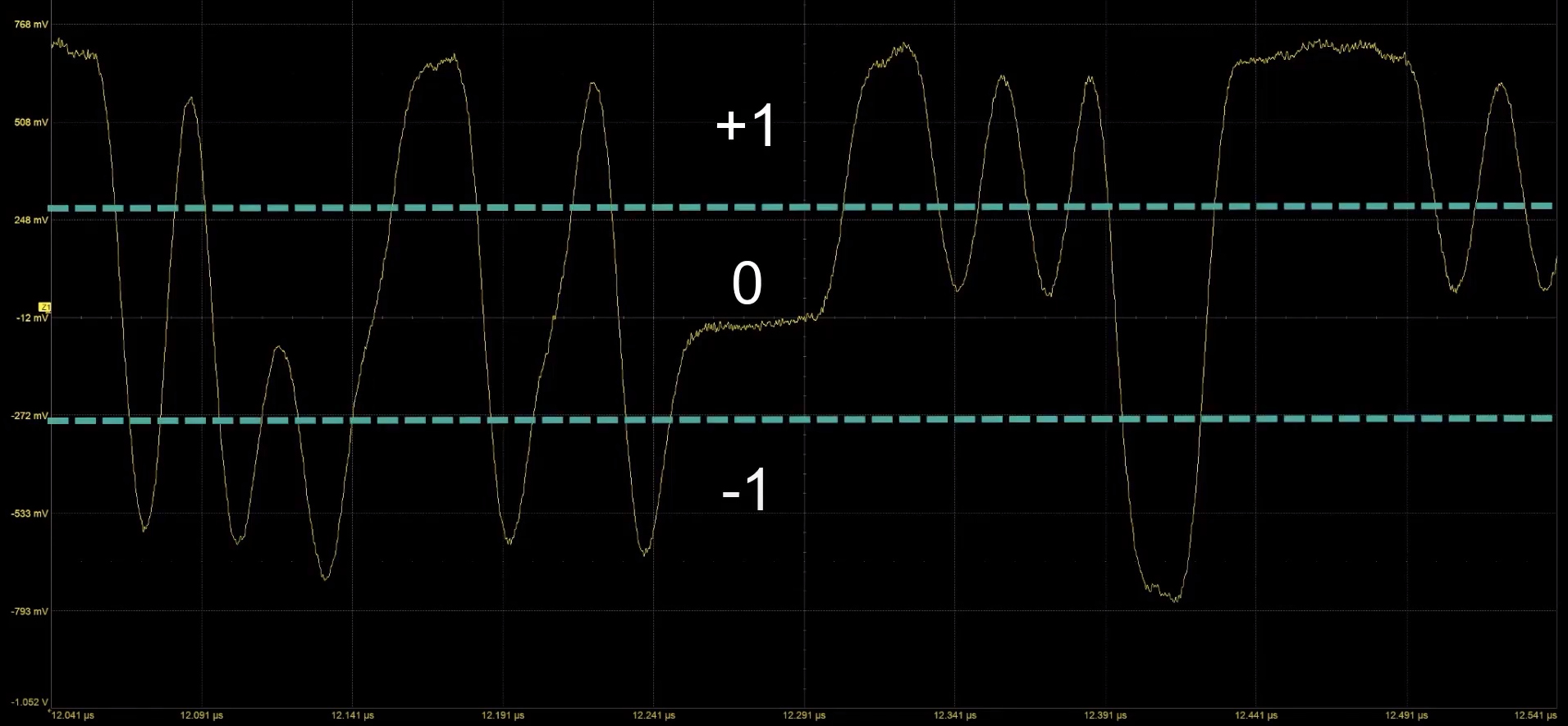
From Teledyne LeCroy on YouTube
PAM-3 is a technology where the data line can carry either a -1, a 0, or a +1. What the system does is actually combine two PAM-3 transmits into a 3-bit data signal, such as 000 is an -1 followed by a -1. This gets complex, so here is a table:
| PAM-3 Encoding | ||
| AnandTech | Transmit 1 |
Transmit 2 |
| 000 | -1 | -1 |
| 001 | -1 | 0 |
| 010 | -1 | 1 |
| 011 | 0 | -1 |
| 100 | 0 | 1 |
| 101 | 1 | -1 |
| 110 | 1 | 0 |
| 111 | 1 | 1 |
| Unused | 0 | 0 |
When we compare NRZ to PAM-3 and PAM-4, we can see the rate of data transfer for PAM-3 is in the middle of NRZ and PAM-4. The reason why PAM-3 is being used in this case is to achieve that higher bandwidth without the extra limitations that PAM-4 requires to be enabled.
| NRZ vs PAM-3 vs PAM4 | |||
| AnandTech | Bits | Cycles | Bits Per Cycle |
| NRZ | 1 | 1 | 1 |
| PAM-3 | 3 | 2 | 1.5 |
| PAM-4 | 2 | 1 | 2 |
PAM-3 has similar limitations to NRZ.

The final line on this image is ‘[something] N6 test-chip focusing on the new PHY technology is working in [the lab and] showing promising results’. That first word I thought was TSMC, but it has to be about the same width as the ‘The’ on the line above. So it doesn’t look like I’m right there, but N6 is a TSMC node.
Intel’s goal with Thunderbolt is going to be both driving bandwidth, power, and utility, but also right now it seems keeping it to the USB-C standard is going to be a vital part of keeping the technology useful for users who can fall back on standard USB-C connections. Right now Intel’s TB4 is a superset that includes USB4, so we might see another situation where TB5 is ready to be a superset of USB5 as well, however it seems that USB standards are slower to roll out than TB standards right now.
Special thanks to David Schor from WikiChip for the tipoff.
Related Reading
- Intel's CES 2021 Press Event: The Future of Intel (A Live Blog, 1pm PT)
- Intel Launches 11th Gen Core Tiger Lake: Up to 4.8 GHz at 50 W, 2x GPU with Xe, New Branding
- Intel Thunderbolt 4 Update: Controllers and Tiger Lake in 2020
- Intel’s 11th Gen Core Tiger Lake SoC Detailed: SuperFin, Willow Cove and Xe-LP
- DisplayPort Alt Mode 2.0 Spec Released: Defining Alt Mode for USB4
- Cypress Announces USB 3.2 & USB4-Ready Controllers: EZ-PD CCG6DF & CCG6SF
- USB 3.2 Gen 2x2 State of the Ecosystem Review: Where Does 20Gbps USB Stand in 2020?


82 Comments
View All Comments
Wereweeb - Monday, August 2, 2021 - link
Good to see that there is still progress being made here.But does anyone know what is the barrier to making optical interconnects cheaper? Why is it so expensive to make optical silicon? Patents? Defect rates? Limited competition in manufacturing?
A5 - Monday, August 2, 2021 - link
Electrical->Optical->Electrical conversion is hard to do and expensive in small form factors. No one is going to make a laptop with an SFP cage on it, for example.Threska - Monday, August 2, 2021 - link
Durability in the face of repeated insertions and removals.mode_13h - Tuesday, August 3, 2021 - link
There's also dirt and dust to contend with.Wereweeb - Tuesday, August 3, 2021 - link
No dirt and dust will get within a sealed Thunderbolt optical cable package, and manufacturing facilities are used to having clean rooms anyway to reduce electrostatic damage.mode_13h - Wednesday, August 4, 2021 - link
If we're talking about cables, you have to consider susceptibility to dirt and wear on both the connector and the socket.Oxford Guy - Thursday, August 12, 2021 - link
The designers of the Fairchild VES were very concerned about the delicacy of circuit boards, so a well-engineered ZIF was designed and deployed.Atari’s VCS engineers went in the opposite direction. Bare circuit boards sticking out of cartridges, cartridges that one forced into the machine and pulled out with force.
Guess which machine was the market success?
Then, there is the utterly odious market success example of the failure of ‘console’ makers to go the DVD-RAM route of producing protected media.
The megacorps involved were far more interested in protecting their IP, via DRM and broken promises (Linux on PS3) than in providing a reliable experience. Root kits. Capacitors that failed due to defective design. RRoD. And so on.
Apple refused to replace the defective GeForce boards in MacBook Pro machines (lead-free solder done incorrectly). Instead, the company would replace one board with another of identically-defective design.
I can continue but reliability for consumers is given short shrift, as it does not feed both planned obsolescence (the thing that really turns tech corporations on) and the speeding of of that.
Really... too... I can’t not mention the wonderful Zip drive.
That there are too many examples of grossly substandard design is one problem. That companies get away with placing most of the burden onto consumers is worse.
mode_13h - Friday, August 13, 2021 - link
Those are all examples of individual companies selling flawed products. For a new cable standard, you'll need a whole consortium of players to buy into this mentality, which seems like more of a reach.And since a lot of device makers aren't in the cable business, they don't want bad/dirty cables causing support calls and returned products. They want cables that "just work".
mode_13h - Tuesday, August 3, 2021 - link
And don't forget about the fragility and cost of high-bandwidth optical cables.Wereweeb - Tuesday, August 3, 2021 - link
Cables are cheap and there are plastic ones available that are pretty good for short distances. The problem is the silicon and package.