Intel's Architecture Day 2018: The Future of Core, Intel GPUs, 10nm, and Hybrid x86
by Dr. Ian Cutress on December 12, 2018 9:00 AM EST- Posted in
- CPUs
- Memory
- Intel
- GPUs
- DRAM
- Architecture
- Microarchitecture
- Xe
Sunny Cove Microarchitecture: A Peek At the Back End
One of the best parts when a new microarchitecture is announced is learning how it all works and how it has changed. Intel has been on close variants of the Skylake core since Skylake first launched in 2015, which has carried through Kaby Lake, Coffee Lake, and Coffee Lake refresh – and so getting an update to his old core design is more than welcome. While I applaud Intel for getting something new to put in front of our faces, the level of information was unfortunately less than complete. For reasons of ‘we’ll discuss more nearer the launch’, Intel was only set on discussing the back end of the microarchitecture design in any detail. In core design parlance, this means everything beyond the dispatch and order queues.
Intel framed its microarchitecture updates into two different sections: general purpose performance increases and special purpose performance increases. The company described the general purpose updates essentially as raw IPC (instructions per clock) throughput or an increase in frequency. An increase in either of these two leads to a performance increase no matter the code, at least as long as it is compute bound. Frequency is often a function of the implementation and process, whereas IPC increases can come from cores being wider (more executing instructions per clock), deeper (more parallelism per clock), and smarter (better data delivery through the front end).

The other type of performance increase is the special purpose kind, which means that certain workloads used in specific scenarios can be improved through additional acceleration methods, such as dedicated IP or specialized instructions.
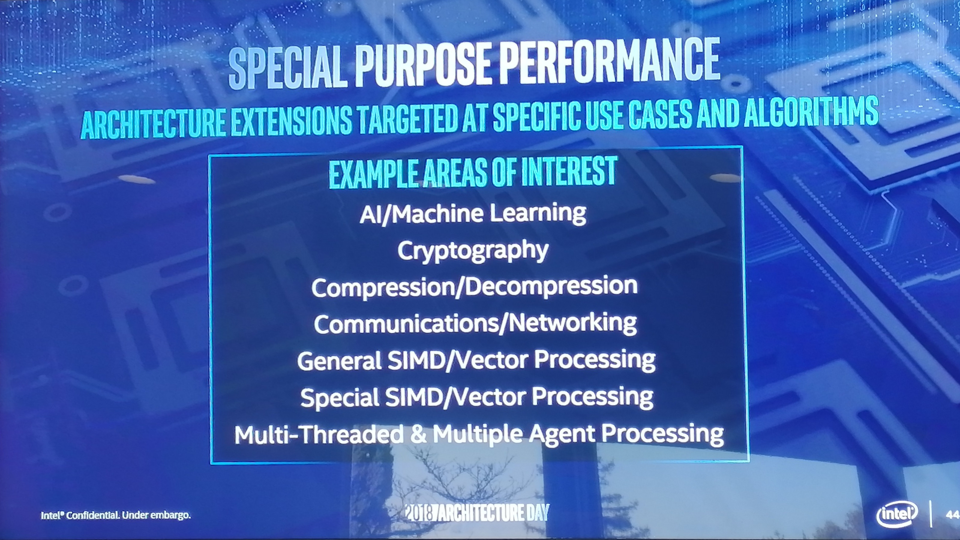
Sunny Cove is set to have both.
On the back end of the microarchitecture design, Intel has done several things including increasing cache sizes, making the execution of the core wider, increasing L1 store bandwidth, and other things.
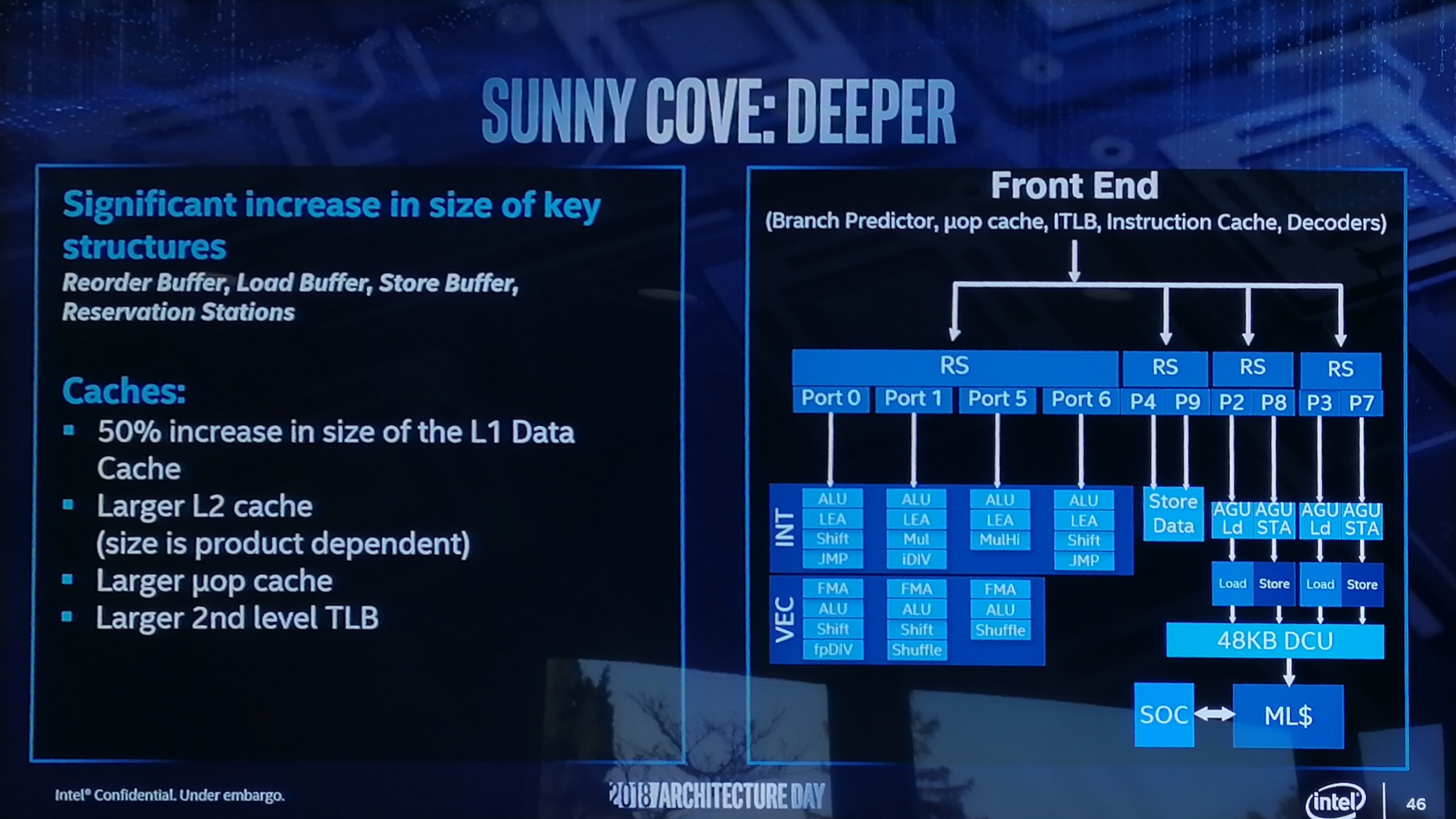
Starting with the cache improvements, the Sunny Cove core back end has a 48 KB L1 Data cache, upgraded from 32 KB. Normally cache misses decrease by a factor of a square root of the proportional size when the cache is increased, so in this case we should expect a 22% reduction in L1-Data cache misses. We are told that the L2 cache size has also been increased in both the Core and Xeon variants of Sunny Cove (256 KB and 1 MB respectively), although to exactly what size will be revealed at a later date.
While not back-end, the micro-op (uOp) cache has increased from a 2048-entry design, although exactly to what Intel is not saying at this point. The second level TLB size has also increased, which will help with machine address translation of recent addresses – normally this is increased when more lookups need to be kept and stored, which means that Intel identified a number of use cases where recent addresses had been evicted shortly before being needed.

From the diagram we can see some other changes, such as the increase in execution ports from eight to ten, allowing more instructions to come out of the schedulers at one time. Port 4 and Port 9 is linked to a cycling data store, doubling that bandwidth, but also the AGU store capabilities have doubled, for which the increased L1-D size will help. Previously on Skylake there was a potential bottleneck when all three AGUs could attempt a store, however only enough bandwidth was present for one per clock cycle. Load performance is unaffected. There is also an allocation increase, moving from four to five. This means that the dispatch out of the reorder buffer can now hit five instructions per cycle, rather than four – however given that the ops/cycle out of the Skylake decoders and uOp cache was four-to-five (depending on certain factors), it will be interesting to see how the front end has changed as a result.
There are also substantial changes in the execution ports between Skylake and Sunny Cove, which is best represented in a diagram and a table:
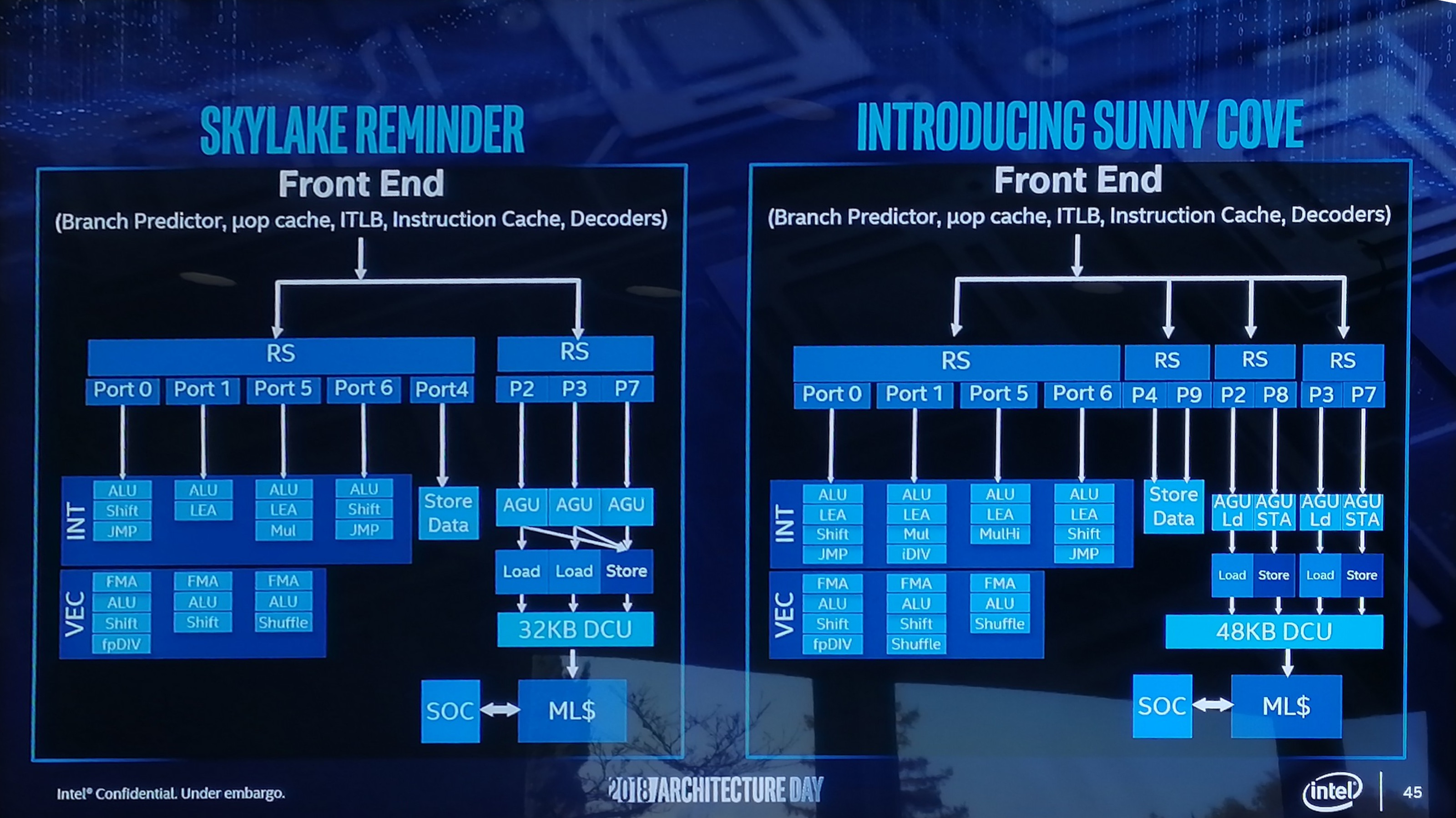
| Back-End Execution Resources | ||||||||
| Skylake | Port | Sunny Cove | ||||||
| Integer | ||||||||
| JMP | Shift | ALU | 0 | ALU | LEA | Shift | JMP | |
| LEA | ALU | 1 | ALU | LEA | Mul | iDIV | ||
| Mul | LEA | ALU | 5 | ALU | LEA | MulHi | ||
| JMP | Shift | ALU | 6 | ALU | LEA | Shift | JMP | |
| Vector / FP | ||||||||
| fpDIV | Shift | ALU | FMA | 0 | FMA | ALU | Shift | fpDIV |
| Shift | ALU | FMA | 1 | FMA | ALU | Shift | Shuffle | |
| Shuffle | ALU | FMA | 5 | FMA | ALU | Shuffle | ||
The parts highlighted in bold are different in the Sunny Cove core.
We see that Intel has equipped the Integer section of the core with more LEA units to help with memory addressing calculations, possibly to help improve performance loss with security mitigations that require frequent memory calculations or to help with high-performance array code with constant offsets. Port 1 gets the Mul unit from Skylake Port 5, probably for rebalancing purposes, but there is also an integer divider unit here. This addition is a bit of a tweak, as we know that Cannon Lake has a 64-bit IDIV unit in its design as well. In that case it brings 64-bit integer division down from 97 clocks (a mix of instructions) down to 18 clocks, and this is likely something similar. Also on the INT side is that Port 5’s multiply unit has become a ‘MulHi’ unit which in other implementations leave most-significant nibble of the result in a register for further use. I'm not sure exactly what its position is here in the Sunny Cove core though.
On the FP side, Intel has increased the shuffle resources, which we are told was because they had customers requesting this functionality to help remove bottlenecks in their code. Intel didn’t state the capabilities for the FMAs in the FP part of the core, however we do know that the core has an AVX-512 unit, so at least one of these FMAs should interface with it. Cannon Lake only has one 512-bit FMA, and that most likely carries over here, and the Xeon Scalable version might get two. I would like to get proved wrong though.
Other updates to the core as listed from Intel include improvements to the branch predictor and a reduced ‘effective load latency’ (due to the TLB and L1-D), although it was pointed out that these improvements won’t help everyone, and might require new algorithms in order to use specific parts of the core.
We’re waiting to see what changes Intel has made on the front-end, which is where a lot of low-hanging fruit often lies for performance.
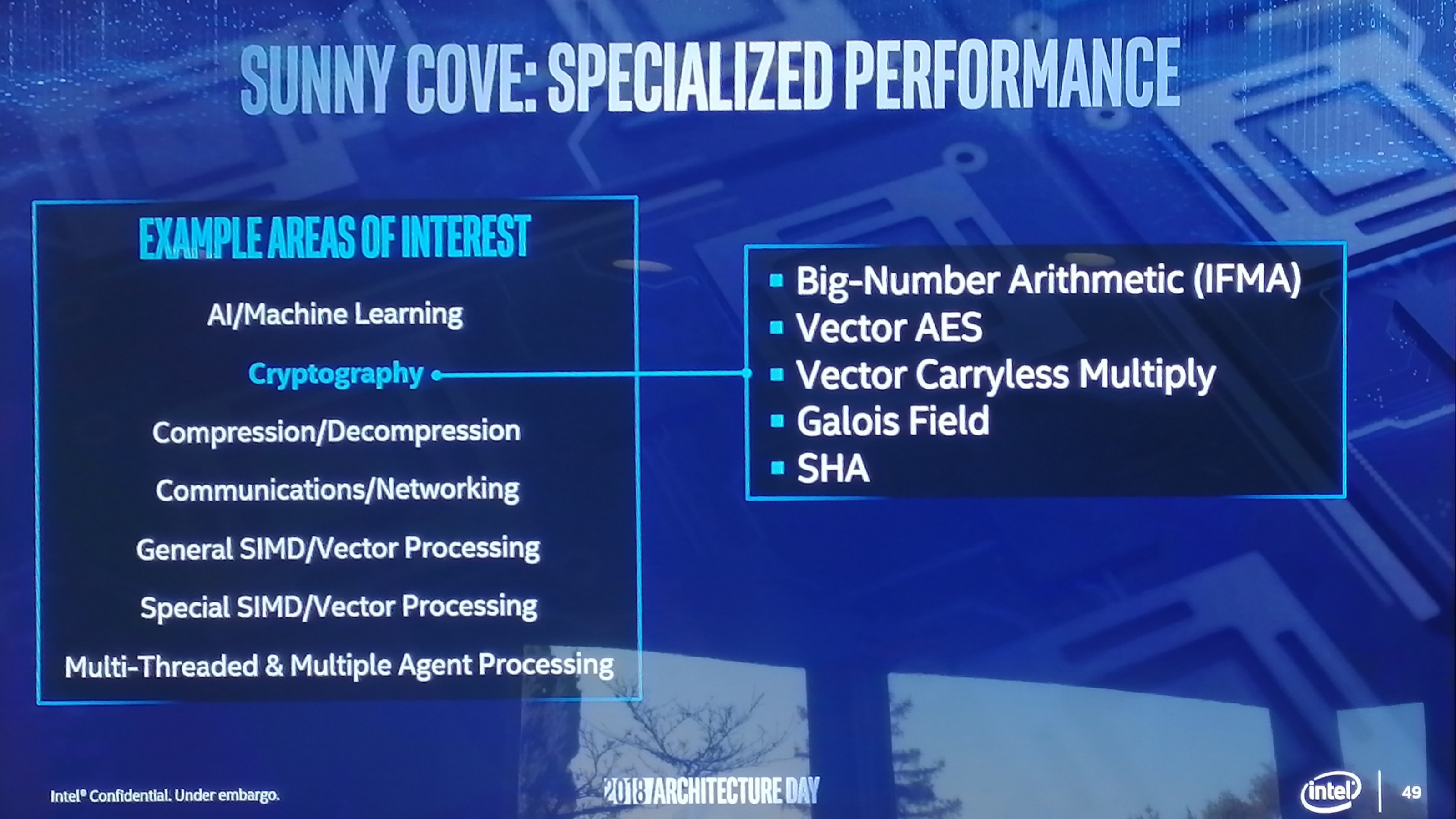
On top of the microarchitecture differences, there are new instructions for the Sunny Cove core to help speed up specialist compute tasks. With the AVX-512 unit in play, the new core will support IFMA instructions for big arithmetic compute, and which are also useful in cryptography. Along the same lines, Vector-AES (supporting more AES concurrently) and Vector Carryless Multiply are also supported. SHA and SHA-NI instructrions are also added, along with Galois Field instructions, which are fundamental building blocks in some elements of cryptography as well.
For Sunny Cove, there is also built-in support for larger memory capacities. The paging table for main memory is now a five layer design, up from four layers, supporting a Linear Address space up to 57 bits and a physical address space up to 52 bits. This means, according to Intel, that the server processors could theoretically support 4 TB of memory per socket. We will see Sunny Cove hit the market in the server space with Ice Lake-SP in 2020 according to Intel’s previous Xeon roadmaps. For security, Sunny Cove has access to Multi-Key Total Memory Encryption, and User Mode Instruction Prevention.
So where does this leave us in terms of Sunny Cove predicted performance compared to Skylake at a clock for clock level? Unfortunately we don’t have enough information. There is only enough to whet the appetite. Intel wants you (and me) to come back for more in 2019.


148 Comments
View All Comments
Raqia - Thursday, December 13, 2018 - link
Your point is taken and Keller did say it was in its infancy, but I am interested in whether what we're seeing here will be a competitive product or will remain an interesting science experiment. There are theoretical benefits of stacking high performance dies on low leakage ones like this but also substantial challenges and deficiencies which the current iteration doesn't show that it has overcome. What we might see in benefit in terms of better overall area, lower package level fab rejection rates, and better net power characteristic could be offset by a worse concentration of heat and hence more throttling when both elements are running or more expensive packaging. Perhaps in the end, a monolithic die is a better compromise despite losing out on some metrics for mobile.nico_mach - Wednesday, December 12, 2018 - link
So the GPU is going to be called ... Ten to the Eeth power? Is that right?I reject all these Xes used in unpredictable ways. The iPhones are pronounced exar and excess. This is ecksee, and I still use oh ess ecks on my emm bee eh at home.
Jon Tseng - Wednesday, December 12, 2018 - link
>Intel actually says that the reason why this product came about is because a customer>asked for a product of about this performance but with a 2 mW standby power state.
Huh wonder who the customer for that Core/Atom hybrid is. Seems a bit overpowered for a tablet. A bit underpowered for a MacBook (or for a car). Chromebooks maybe but most are too low volume to demand a custom part (maybe the education market is taking off?). PC OEMs don't normally take such custom parts for their laptops. But the graphics loadout implies some kind of PC-type application?
Any ideas??
HStewart - Wednesday, December 12, 2018 - link
From the diagram, it appears that hybrid cpu - has single Core CPU with 4 small (Atom) CPU's - such technology is done with Samsung Processors - this would mean it still lower power - but still have primary single thread core speed.Most interesting would be how the smaller core are used in scheduling system. Most like means and enhancement in OS for proper usage.
A5 - Wednesday, December 12, 2018 - link
There aren't a ton of companies big enough to make Intel create a new product line just for them.The whole list is probably Apple/HP/Dell. Maybe Microsoft.
The_Assimilator - Wednesday, December 12, 2018 - link
Microsoft Surface, obviously. It's become a very profitable line for MS but the current models are either too battery-hungry (Core CPUs) or too slow (Atom CPUs). Fovoros will give the best of both these worlds while also being x86... priced right, a Fovoros-based Surface will essentially end any argument for iPads in a business environment, especially considering most software remains firmly single-threaded. But it remains to be seen whether (a) Intel can get the power down even further (7W is still double most smartphones) and (b) whether their big.LITTLE implementation is good enough.Raqia - Wednesday, December 12, 2018 - link
Windows on ARM will do just fine now that Visual Studio emits ARM native code. Once Chrome gets ported (and that will be soon https://www.neowin.net/news/both-chromium-and-fire... the platform should address 95% of typical daily use cases and provide substantial compatibility with legacy software / file formats. This is better value than iPads and upcoming dedicated SoCs like the 8cx should offer better performance and battery / heat characteristics than what Intel has planned for next year in the same power envelope.The_Assimilator - Thursday, December 13, 2018 - link
I think you missed the part where Windows on ARM is horribly slow and therefore shitty. As a result, Microsoft has no plans to port anything useful (e.g. Office) to ARM, which means Windows on ARM is stuck being the lowest of the low-end. And that's not a space that Surface is intended to play in; Surface is an iPad competitor, and an iPad competitor can't be slow and shitty. Business devices can't be slow and shitty, and they absolutely need to be able to run Office.I expect that either Windows on ARM will be allowed to wither and die once Fovoros ships, or it will languish in a dead zone whereby only the cheapest of the cheap devices by no-name-brand OEMs (think $100 Lenovo tablets) use ARM chips and hence need it.
So unless Qualcomm's 8cx is a game-changer in terms of performance, Fovoros should be the end of ARM on desktop, and thank fucking God for that.
Spunjji - Thursday, December 13, 2018 - link
Microsoft already have an Office code base on ARM, so I'm not sure what you're talking about there.What would worry me about an Intel BIG.little style design is that if Windows doesn't assign your performance-critical application to the correct (big) core, performance will mostly suck just as hard as if all your cores were Atom.
As such, I'd be cautious on calling a winner just yet.
gamerk2 - Thursday, December 13, 2018 - link
Agreed with this; Microsoft has been let down by Intel not having a good mobile platform. If it were up to them, they wouldn't bother with ARM, but they have to due to battery/power/heat requirements.