GlobalFoundries Stops All 7nm Development: Opts To Focus on Specialized Processes
by Anton Shilov & Ian Cutress on August 27, 2018 4:01 PM EST- Posted in
- Semiconductors
- CPUs
- AMD
- GlobalFoundries
- 7nm
- 7LP
GlobalFoundries on Monday announced an important strategy shift. The contract maker of semiconductors decided to cease development of bleeding edge manufacturing technologies and stop all work on its 7LP (7 nm) fabrication processes, which will not be used for any client. Instead, the company will focus on specialized process technologies for clients in emerging high-growth markets. These technologies will initially be based on the company’s 14LPP/12LP platform and will include RF, embedded memory, and low power features. Because of the strategy shift, GF will cut 5% of its staff as well as renegotiate its WSA and IP-related deals with AMD and IBM. In a bid to understand more what is going on, we sat down with Gary Patton, CTO of GlobalFoundries.
7LP Canned Due to Strategy Shift
GlobalFoundries was on track to tape out its clients’ first chips made using its 7 nm process technology in the fourth quarter of this year, but “a few weeks ago” the company decided to take a drastic, strategic turn, says Gary Patton. The CTO stressed that the decision was made not based on technical issues that the company faced, but on a careful consideration of business opportunities the company had with its 7LP platform as well as financial concerns.
It is noteworthy that when GlobalFoundries first announced its 7LP platform in September 2016, it said that it would start risk production of processors using this technology in early 2018 (PR), which means that the first chips should have been taped out before that. When the company detailed the process in June 2018, it said that it expected to start “volume production ramping in the second half of 2018” (PR), which would be close to impossible if customers taped out their first chips only in Q4.
Generally, it looks like the company had to adjust its roadmap somewhere along the way, moving the start of high-volume manufacturing (HVM) further into 2019. Whether or not these adjustments had any implications on GlobalFoundries is up to debate. Keep in mind that AMD’s first 7 nm product was designed for TSMC’s CLN7FF from the beginning, so the company did not bet on GF’s 7LP in late 2018 anyway, and no rush with the manufacturing technology was needed for GF’s key customer.
Along with the cancellation of the 7LP, GlobalFoundries essentially canned all pathfinding and research operations for 5 nm and 3 nm nodes. The company will continue to work with the IBM Research Alliance (in Albany, NY) until the end of this year, but GlobalFoundries is not sure it makes sense to invest in R&D for ‘bleeding edge’ nodes given that it does not plan to use them any time soon. The manufacturer will continue to cooperate with IMEC, which works on a broader set of technologies that will be useful for GF’s upcoming specialized fabrication processes, but obviously it will refocus its priorities there as well (more on GF’s future process technologies later in this article).
So, the key takeaway here is that while the 7LP platform was a bit behind TSMC’s CLN7FF when it comes to HVM – and GlobalFoundries has never been first to market with leading edge bulk manufacturing technologies anyway – there were no issues with the fabrication process itself. Rather there were deeper economic reasons behind the decision.
![]()
Economic Reasons Behind the Move
As we noted in our article covering GlobalFoundries's new CEO hire earlier this year, former CEO Sanjay Jha was never able to make the company profitable. His key tasks were to increase GlobalFoundries’s sales, streamline the company in general, and ensure that it executes its roadmap.
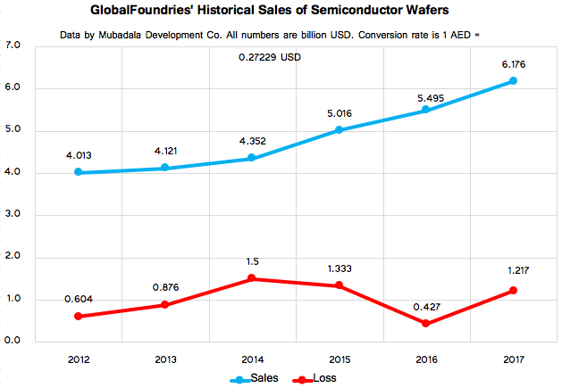
To address the needs of the manufacturer’s traditional key client (AMD) and ensure that his company was competitive against other contract makers of semiconductors, he licensed Samsung Foundry's 14LPP fabrication technology. That strategy worked well. With Sunjay Jha at the helm, GlobalFoundries has managed to land a variety of new customers and increase its sales of semiconductor wafers from approximately $4.121 billion in 2013 to $6.176 billion in 2017. Besides, the foundry’s leading-edge Fab 8, which has been processing wafers using exclusively 14LPP process technology for well over 1.5 years now, is running at full capacity.
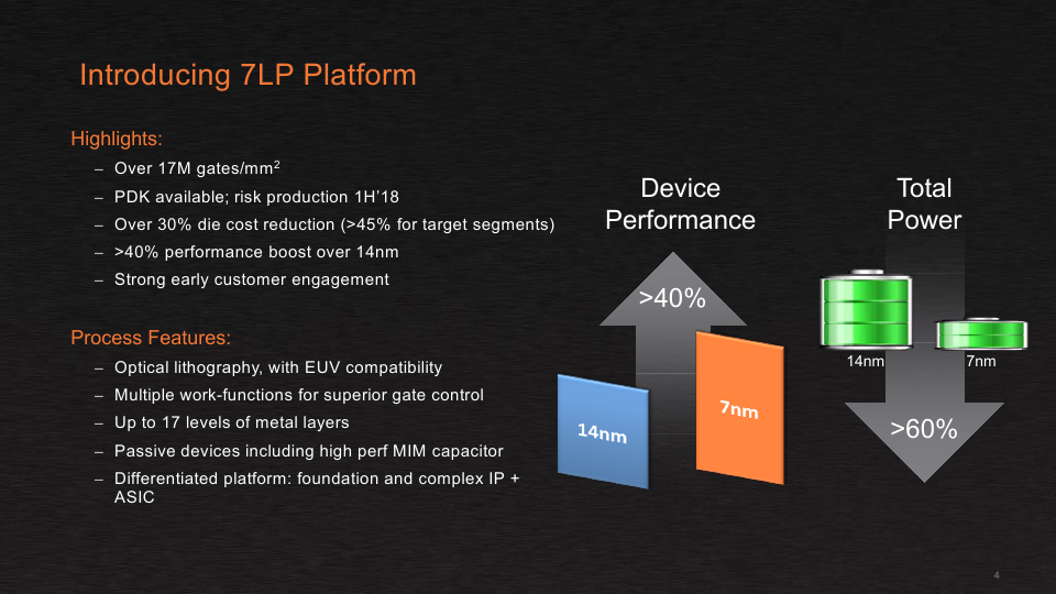
To ensure that GlobalFoundries remains competitive against Samsung Foundry and TSMC in the long run, Sunjay Jha obtained IP and development teams from IBM (along with two fabs and a lot of obligations), and poured in billions of dollars in development of the 7LP fabrication technology platform. The latter would include three generations of manufacturing processes and, possibly, a custom high-performance technology available exclusively to IBM. While everything appeared to proceed smoothly with the 1st Gen 7 nm process (DUV only), the 2nd Gen 7 nm process (with EUV used for non-critical layers, such as padding) still needed some additional development investments, and the 3rd Gen 7 nm (with intensive usage of EUV) required even more money for development and further could require installation of additional EUV equipment. Meanwhile, there were two things to consider.
First. If GlobalFoundries kicks off production using the 1st Gen 7 nm fabrication process, it would have needed to cure all of its teething troubles and offer its clients a roadmap forward. The latter would have included 2nd Gen and 3rd Gen 7 nm, but nothing stops there. Customers would have asked for 5 nm and then for 3 nm nodes. Meanwhile, you cannot tell your clients that you are packing up after a certain node and then hope that this node will be a success (the same is true for DUV-only 1st Gen 7 nm).
Second. Development of leading-edge process technologies is extremely expensive. Every new node requires billions of dollars in investments. Those costs are eventually amortized over each chip the company makes, so to keep increasing R&D costs from driving up chip prices, foundries need to produce more chips. To make more chips, they need to either run multiple fabs that use the same process technology (these are going to cost $10+ billion in the EUV era), or build giant fabs that process a gargantuan number of wafers (these are going to cost $20+ billion in the EUV era). Meanwhile, GlobalFoundries has only one leading-edge fab featuring capacity of 60,000 wafer starts per month. As a result, either GlobalFoundries has to pass these R&D costs on to the finite number of wafers it processes – and become uncompetitive against rivals in the process – or eat the costs with reduced profitability.
Meanwhile, having spent well over $20 billion on GlobalFoundries over the last 10 years, Mubadala, the owner of the company, is not inclined to lose more money or invest tens of billions in the hopes of becoming profitable one day. The investor wants GlobalFoundries to stop bleeding and start generating profits.
“The culture of [our investments], the ones I’ve been involved with, was about accumulating assets and then just maintaining it,” said Mubadala CEO Khaldoon Al Mubarak in an interview with Bloomberg earlier this year. “The shift that has happened over the last couple of years, that I’ve tried to push at Mubadala today, is a monetization strategy that makes sense, not with a view to cash out but with a view to reinvest.”
Gary Patton admits that GlobalFoundries never planned to be a leading producer of 7-nm chips in terms of volume. Furthermore, the company has been seeing increasing adoption of its 14LPP/12LP technologies by designers of various emerging devices, keeping Fab 8 busy and leaving fewer step-and-scan systems for 7LP products.
Without another big fab, it would be impossible to make any new leading-edge process technology competitive against Samsung and TSMC due to aforementioned scale reasons. Meanwhile, building a new fab (or even expanding the Fab 8 with another clean room module, which is something that GF considered several years ago) and creating another node or two would require another $10 – $15 billion from Mubadala, which is not inclined to invest just now. As a result, the GlobalFoundries has decided to switch entirely to specialized process technologies for emerging high-growth markets. This strategic shift enables it to reduce spending on R&D, slowdown procurement of new equipment, reduce its workforce by 5% (most of which will be in Malta), and potentially avoid direct competition against the aforementioned contract makers of semiconductors.


127 Comments
View All Comments
haukionkannel - Tuesday, August 28, 2018 - link
Zen2 is in no trouble. Vegas most likely and APUs were planned to use Global foundaries, so those may be delayed one or two years. Or They will stay in 14nm for some years. No big deal.GreenReaper - Tuesday, August 28, 2018 - link
It kind of is? Heat and power use are bad in themselves and limit the frequency you can reach; die size also relates closely to cost. For APUs, you don't need more cores, but increasing the number of compute and rendering units could be the difference between reaching 4K or not.Sure, you can make that die on 14nm, but you will pay for it one way or another. Maybe thanks to size or power it doesn't fit into an AM4 socket at all, and you need to go to TR4.
OwCH - Tuesday, August 28, 2018 - link
This is actually a really smart move.To all the people calling for a move away from Si - Tell that to Intel, Samsung and TSMC, as those three will be the ones leading development of new nodes. For the vast majority of tech products, we don't need those smaller/faster nodes. Think IoT and normal household tech. The bulk of tech. The need for computing power in a single chip isn't huge for that market. For that market we need a reliable, efficient, profitable and cheap node. 40nm, 22nm and 14nm can do just that. GF fabs them all. Smart move.
spronkey - Tuesday, August 28, 2018 - link
Smart short term move, but increasing the chances they'll fade into oblivion as their tech can't compete in the longer term. 7nm will be extremely appealing to IoT in 5-10 years once it's reasonably cheap.Doesn't really sound like they had a choice though.
BurntMyBacon - Tuesday, August 28, 2018 - link
Just because they are focusing on non-bleeding edge nodes doesn't mean they won't revisit 7nm when it is no longer bleeding edge. 7nm fabrication will likely be cheaper by the time 3nm is ramping up. At the very least, they could skip DUV with quadruple masking and go straight to EUV allowing them to make more wafer starts with the same amount of production space.zodiacfml - Tuesday, August 28, 2018 - link
Right. They don't have a choice. It is quite puzzling they are withdrawing quite late.I think there is a change with their competitors. It seems that TSMC must have been giving better prices for contracts. It also seems that TSMC can serve all customers as long they are willing to wait.
In short, GF lost some potential customers making the latest node not worth it
MananDedhia - Tuesday, August 28, 2018 - link
It is sad to read this news - i worked at Fab 8 for 3 years and know the struggles involved in developing bleeding edge processes first hand, especially at the brutal timelines that are demanded from the market. Hopefully people affected by this action manage to find work elsewhere.Crazyguy9 - Tuesday, August 28, 2018 - link
Good points by the commenters, but I think many miss the main point. Yes, we all know and have known how expensive new nodes are to develop. And we all have known how crazy it can be to chase Moore’s Law. BUT, so did Global. They must have had a business plan when they launched 7nm two years ago. They knew how much capital it would take, how much it would cost to make a wafer, and how much revenue they could make. They spent billions of dollars on development and tools like EUV over the last two years. According to their press releases they should be ready for production this year. So why do you cancel it now ??? Something doesn’t add up. Think of how much it must have cost to outfit the fab for EUV tools alone.Yes there is a lot of demand for older nodes like 28nm. But 28nm was the end of the line for planer devices and finfet arrival was delayed several years. In contrast, 14nm is first generation finfet and probably not a good place to park a fab.
So there must be more to this story than just “we woke up and discovered how expensive these new nodes are”. Something is very amiss at Global to get this far down the road, then cancel.
V900 - Tuesday, August 28, 2018 - link
It’s Global Foundries...Hardly the best managed company out there, and not exactly known for their sterling leadership and flawless execution.
They also had huge problems transitioning to previous nodes.
Having said that, it’s kinda like a gambler who already lost his paycheck, and is about to throw the deed to his house on the table.
YES, GF already lost 5-7 billion dollars researching 7nm, investing in EUV tools etc.
But continuing the move to 7nm would have cost them an additional 10-20 billion dollars.
And that investment might never have paid for itself, since GF in 5 years might have been stuck with a 7 nm fab that’s too slow for the leading edge (Apple, Qualcomm etc.) but too expensive for everyone else compared with a cheap “good enough” 14nm or 22nm fab.
del42sa - Thursday, August 30, 2018 - link
no it would cost them a lot of less :It would have cost GF $2-4 billion to ramp up the 40-50,000 wafers/month capacity needed to have a chance of making a return on the node. “
https://www.eetimes.com/document.asp?doc_id=133363...