The Intel Skylake-X Review: Core i9 7900X, i7 7820X and i7 7800X Tested
by Ian Cutress on June 19, 2017 9:01 AM ESTThe Basin Falls Platform: X299, SKL-X, & KBL-X
For most practical definitions of the Basin Falls platform, the X299 chipset is the heart. X299 supports the new processors, and like the Z170 and Z270 counterparts on the mainstream consumer line, is basically a big PCIe switch. One of the issues with the older X99 chipset was its limited capabilities, and inability to drive many PCIe devices – this changes with the big switch mentality on X299. For the DMI 3.0 link going into the chipset (basically a PCIe 3.0 x4), the chipset has access to up to 24 PCIe 3.0 lanes for network controllers, RAID controllers, USB 3.1 controllers, Thunderbolt controllers, SATA controllers, 10GbE controllers, audio cards, more PCIe slot support, special controllers, accelerators, and anything else that requires PCIe lanes in either an x4, x2 or x1 link. The total uplink is limited by the DMI 3.0 link, but there will be very few situations where this is saturated. There are a few limits to what support is available (some ports are restricted in what they can handle), and only three PCIe 3.0 x4 drives can use the in-built PCIe RAID, but this should satiate all but the most hardcore enthusiasts.
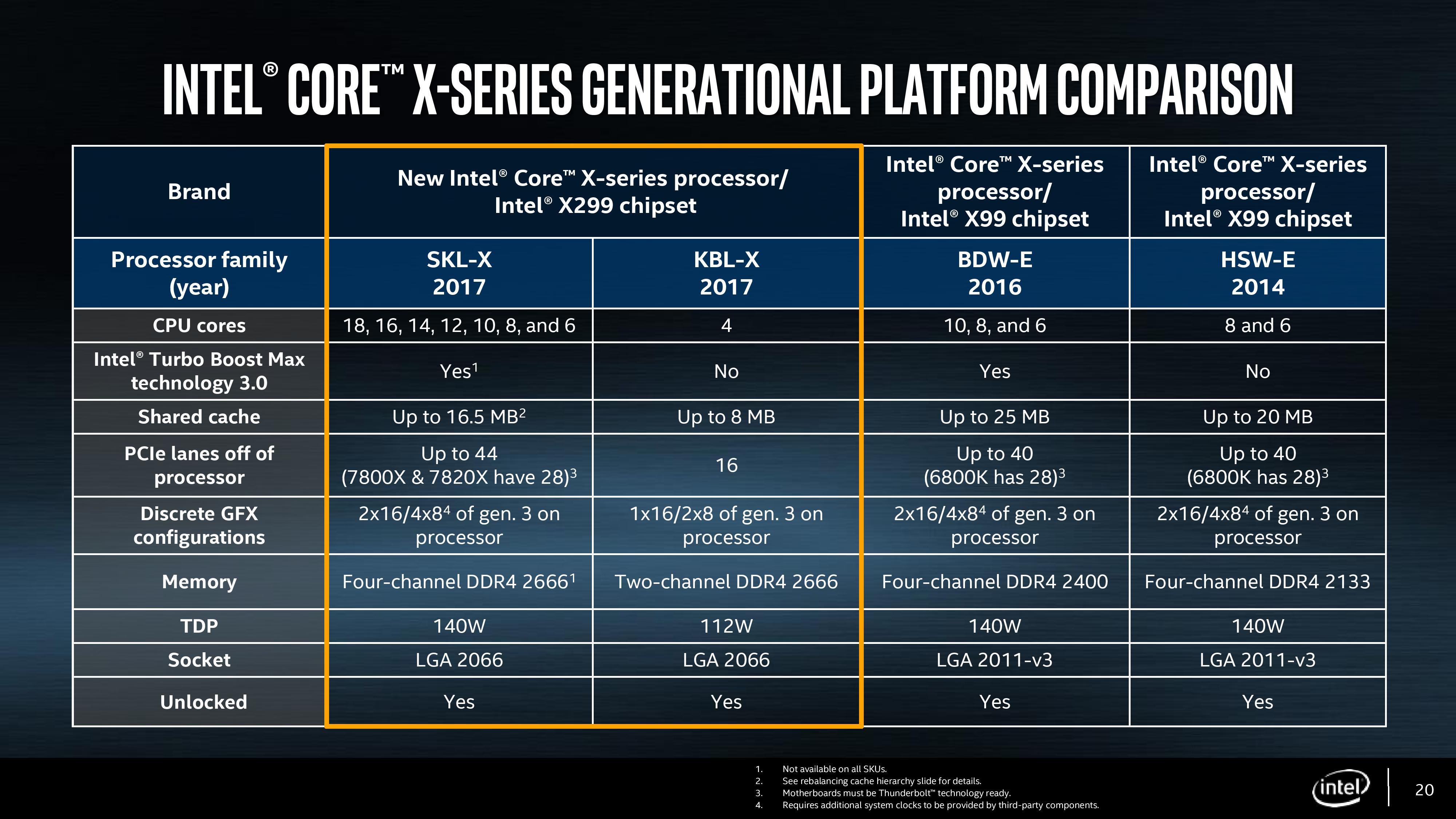
The Skylake-X family of processors for Basin Falls comes in two stages, based on the way the processors are developed. Normally HEDT processors are cut down versions of enterprise processors, usually through restricting certain functions, but the enterprise processors are typically derived from three different silicon layouts during manufacturing. Internally Intel call these three layouts the LCC (low core-count), HCC (high core-count) and XCC (extreme core-count), based on the maximum number of cores they support. Nominally Intel does not disclose which silicon layout they use for which processors, though it is usually straight forward to work them out as long as Intel has disclosed what the configurations of the LCC/HCC/XCC dies are. In this case, Intel has officially left everyone guessing, but the point here is that historically Intel only uses the LCC silicon from the enterprise line for its consumer desktop processors.
In previous generations, this meant either a 6, 8 or 10 core processor at the top of the stack for consumers, with lower core count models being provided by binning/salvaging imperfect CPUs. Each year we expected one of two things: the top-end SKU either gets more frequency, less power, or more cores, and as such the march of progress has been predictable. If you had asked us two months ago, we would have fully expected Skylake-X to top out with LCC silicon at 10 or 12 cores, depending on how Intel was planning the manufacturing part.
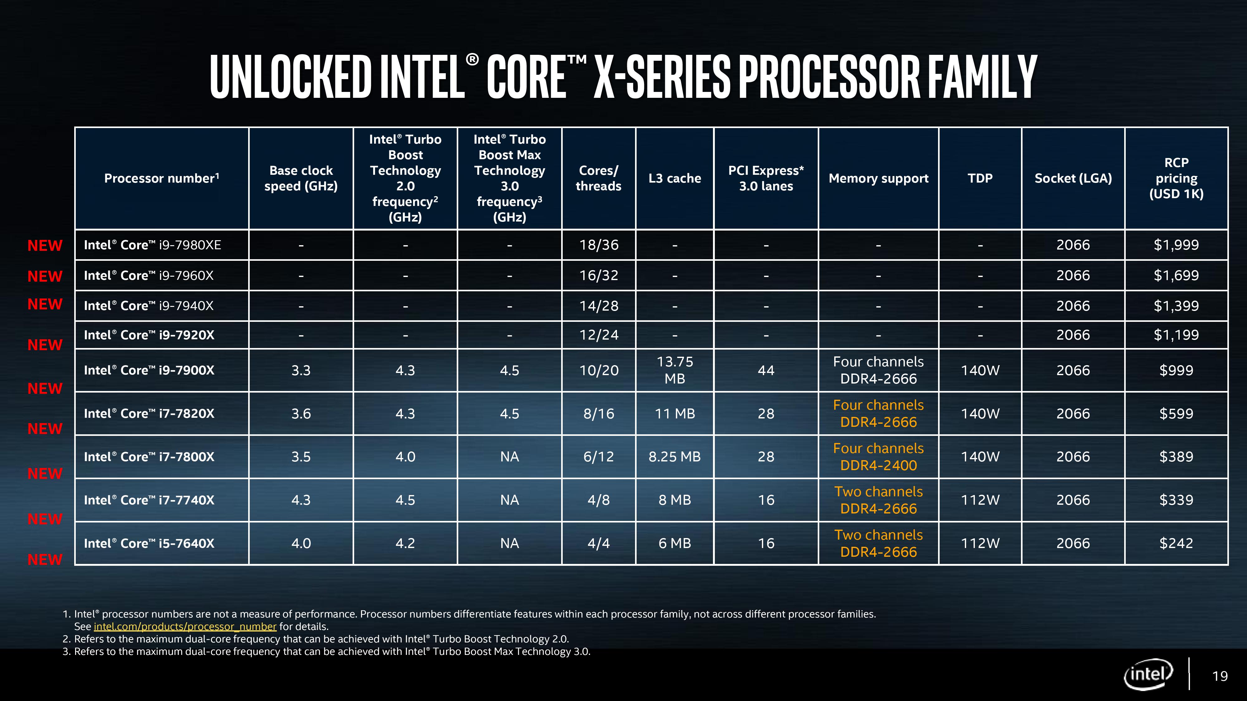
So the first element of Intel’s launch is the LCC processors, running up to 10 cores. We previously published that the LCC silicon was 12 cores, but we can now show it is 10 – more on that later. The three Skylake-X CPUs launching today are using LCC silicon with 6, 8 or 10 cores as the Core i7-7800X, Core i7-7820X and Core i9-7900X respectively. Intel is further separating these parts by adjusting the level of official supported DRAM frequency, as well as the PCIe lanes. We’ll go in a bit more detail further in the review.
The second element to the Skylake-X launch is the one that has somewhat surprised most of the industry: the launch will contain four processors based on the HCC silicon. Technically these processors will not be out until Q4 this year (one SKU coming out in August), and the fact that Intel did not have frequency numbers to share when announcing these parts shows that they are not finalized, calling into question when they were added to the roadmap (and if they were a direct response to AMD announcing a 16-core part for this summer). We’ve written a detailed analysis on this in our launch coverage, and we’ll cover some of the topics in this review. But Intel is set to launch 12, 14, 16 and 18-core consumer level processors later this year, with the top part running a tray price (when you buy 1k CPUs at a time) of $1999, so we expect the retail to be nearer $2099.
It should be noted that due to a number of factors, the Skylake-X cores and the communication pathways therein are built slightly differently to the consumer version of Skylake-S, which is something discussed and analyzed in this review.
The final element to the Basin Falls launch is Kaby Lake-X. This is also an aspect of the Basin Falls platform that deviates from the previous generations. Intel’s HEDT line has historically been one generation behind the mainstream consumer platform due to enterprise life cycles as well as the added difficulty of producing these larger chips. As a result, the enterprise and HEDT parts have never had the peak processing efficiency (IPC, instructions per clock) of the latest designs and have sat in the wings, waiting. By bringing the Kaby Lake microarchitecture to HEDT, this changes the scene, albeit slightly. Rather than bringing a new big core featuring the latest microarchitecture, Intel is repurposing the Kaby Lake-S mainstream consumer silicon, binning it to slightly more stringent requirements for frequency and power, disabling the integrated graphics, and then putting it in a package for the high-end desktop platform. There are still some significant limitations, such as having only 16 PCIe 3.0 lanes and dual channel memory, which might exclude it from the traditional designation of being a true HEDT processor, however Intel has stated that these parts fill a request from customers to have the latest microarchitecture on the HEDT platform. They also overclock quite well, which is worth noting.
The Kaby Lake-X parts will consist of a Core i7 and Core i5, both of which are quad core parts, with the i7 supporting hyperthreading. We have a parallel Kaby Lake-X review alongside our Skylake-X coverage, with some numbers from a stable 5 GHz overclock.


264 Comments
View All Comments
Slappi2 - Monday, June 19, 2017 - link
Running 1080s, doubt I'll notice.Luckz - Monday, June 19, 2017 - link
That's an impressive review / article considering the source.prophet001 - Monday, June 19, 2017 - link
The TDP on the chip is 140W. If they can't cool it then there's a problem with the heat spreader.How well it overclocks is another point of discussion separate from this one.
prisonerX - Monday, June 19, 2017 - link
And yet the only reason you're seeing it at all is becuase of AMD. You epitomise the pure, untrammeled genius of typical Intel customers.Spunjji - Tuesday, June 20, 2017 - link
This is lost on Slappi.FreckledTrout - Monday, June 19, 2017 - link
Slappi2, you reading the same charts? Also have you seen game reviews on other sites. The 1800x holds its own pretty well compared to t he 7820x 8-core, yes the 7820x is faster but not by a huge margin. We don't have Thredripper just yet to see AMD's 10 core comparison so saying Intel's 10 core is killing AMD's 8-core models is a bit disingenuous.AnandTechReader2017 - Monday, June 19, 2017 - link
The review is missing power consumption, clock speed and current price.At no point is it stated what clock speed anything is running at, it could be that Ryzen is running at base and Intel running overclocked (as speedshift would allow). There are also no comparisons with speedshift on/off.
There is no mention of power draw, the Intel processors are all using a 112/130/140W envelope, but are probably way below that with base, while Ryzen is 95/65W with no mention if overlocked above that envelope or underclocked.
If you check Amazon, one can get the R7 1800X for $439 versus the $499 they posted.
Also, the top Intel chips are competing with Thread Ripper, not Ryzen 7.
You're probably going to accuse me of fanboyism, I just don't like it if so many test details are missing. There is also no mention of temperature at max load, etc.
AnandTechReader2017 - Monday, June 19, 2017 - link
To add: They also have 2666MHz and 3000MHz RAM, yet they don't state what clock speed the test is run at.There is so much information missing.
Ian Cutress - Monday, June 19, 2017 - link
Power consumption is added. Sorry, I'm currently half-way around the world suffering jet lag - I had the graph compiled, I just forgot to write about it. It's been added.Clock Speed: As per the first page.
Current Pricing: As per the first page.
With regards the recent price drops from AMD on the Ryzen chips - everything seems to point that this is distributor driven. We've not seen anything official from AMD (such as price lists) that confirm an official price drop. If you have a link to that, please share.
On the DRAM: our standard policy as with every review is to run JEDEC for the maximum officially supported frequency. Nothing changes in this review. So that's DDR4-2666 for the 7900X and 7820X, and DDR4-2400 for the 7800X.
Tamz_msc - Monday, June 19, 2017 - link
What benchmark was used for the power consumption data?