InFO
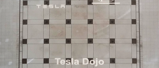
TSMC has been offering its System-on-Wafer integration technology, InFO-SoW, since 2020. For now, only Cerebras and Tesla have developed wafer scale processor designs using it, as while they have fantastic performance and power efficiency, wafer-scale processors are extremely complex to develop and produce. But TSMC believes that not only will wafer-scale designs ramp up in usage, but that megatrends like AI and HPC will call for even more complex solutions: vertically stacked system-on-wafer designs. Tesla Dojo's wafer-scale processors — the first solutions based based on TSMC's InFO-SoW technology that are in mass production — have a number of benefits over typical system-in-packages (SiPs), including low-latency high-bandwidth core-to-core communications, very high performance and bandwidth density, relatively low power delivery network impendance, high performance efficiency, and redunancy. But...
TSMC: We Want OSATs to Expand Their Advanced Packaging Capability
Almost since the inception of the foundry business model in the late 1980s, TSMC would produce silicon. In contrast, an outsourced semiconductor assembly and test (OSAT) service provider would...
2 by Anton Shilov on 10/16/2023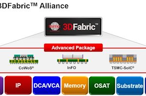
TSMC to Build $2.87 Billion Facility For Advanced Chip Packaging
TSMC on Tuesday announced plans to construct a new advanced chip packaging facility in Tongluo Science Park. The company intends to spend around $2.87 billion on the fab that...
3 by Anton Shilov on 7/25/2023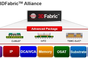
TSMC Opens Advanced Backend Packaging Fab for AI and HPC Products
TSMC on Friday formally opened its Advanced Backend Fab 6 facility, which it will be using to expand the company's capacity for building high-end, multi-chiplet products. The facility is...
1 by Anton Shilov on 6/9/2023
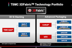
TSMC Forms 3DFabric Alliance to Accelerate Development of 2.5D & 3D Chiplet Products
Currently the majority of high-end processors are monolithic, but design methodologies are slowly but surely shifting to multi-chiplet modules as leading-edge fabrication technologies get more expensive to use. In...
9 by Anton Shilov on 10/27/2022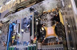
As HPC Chip Sizes Grow, So Does the Need For 1kW+ Chip Cooling
One trend in the high performance computing (HPC) space that is becoming increasingly clear is that power consumption per chip and per rack unit is not going to stop...
40 by Anton Shilov on 6/27/2022
3DFabric: The Home for TSMC’s 2.5D and 3D Stacking Roadmap
Interposers. EMIB. Foveros. Die-to-die stacking. ODI. AIB.TSVs. All these words and acronyms have one overriding feature – they are all involved in how two bits of silicon physically connect...
9 by Dr. Ian Cutress on 9/2/2020


