The Intel SSD DC S3700: Intel's 3rd Generation Controller Analyzed
by Anand Lal Shimpi on November 5, 2012 12:01 PM EST- Posted in
- Cloud Computing
- Storage
- IT Computing
- SSDs
- Intel
Today Intel is announcing its first SSD based on its own custom 6Gbps SATA controller. This new controller completely abandons the architecture of the old X25-M/320/710 SSDs and adopts an all new design with one major goal: delivering consistent IO latency.
All SSDs tend to fluctuate in performance as they alternate between writing to clean blocks and triggering defrag/garbage collection routines with each write. Under sequential workloads the penalty isn't all that significant, however under heavy random IO it can be a real problem. The occasional high latency blip can be annoying on a client machine (OS X doesn't respond particularly well to random high IO latency), but it's typically nothing more than a rare hiccup. Users who operate their drives closer to full capacity will find these hiccups to be more frequent. In a many-drive RAID array however, blips of high latency from each drive can destructively work together to reduce the overall performance of the array. In very large RAID arrays (think dozens of drives) this can be an even bigger problem.
In the past, we've recommended simply increasing the amount of spare area on your drive to combat these issues - a sort of bandaid that would allow the SSD controller to better do its job. With its latest controller, Intel tried to solve the root cause of the problem.
The launch vehicle for Intel's first 6Gbps SATA controller is unsurprisingly a high-end enterprise drive. Since the 2008 introduction of the X25-M, Intel has shifted towards prioritizing the enterprise market. All divisions of Intel have to be profitable and with high margins. The NAND Solutions Group (NSG) is no exception to the rule. With consumer SSDs in a race to the bottom in terms of pricing, Intel's NSG was forced to focus on an area that wouldn't cause mother Intel to pull the plug on its little experiment. The enterprise SSD market is willing to pay a premium for quality, and thus it became Intel's primary focus.
The first drive to use the new controller also carries a new naming system: the Intel SSD DC S3700. The DC stands for data center, which bluntly states the target market for this drive. While it's quite likely that we'll see a version appear in a high-end drive that could be used in a desktop, I don't know that we'll see a mobile version anytime soon for reasons I'll get to later.
The Drive
The S3700 comes in four capacities (100, 200, 400 and 800GB) and two form factors (2.5" and 1.8"). The 1.8" version is only available at 200GB and 400GB capacities. Intel sees market potential for a 1.8" enterprise SSD thanks to the increasing popularity of blade and micro servers. The new controller supports 8 NAND channels, down from 10 in the previous design as Intel had difficulty hitting customer requested capacity points at the highest performance while populating all 10 channels.
The S3700 is a replacement to the Intel SSD 710, and thus uses Intel's 25nm MLC-HET (High Endurance Technology) NAND. The S3700 is rated for full 10 drive writes per day (4KB random writes) for 5 years.
| Intel SSD DC S3700 Endurance (4KB Random Writes, 100% LBA) | ||||||
| 100GB | 200GB | 400GB | 800GB | |||
| Rated Endurance | 10DW x 5 years | 10DW x 5 years | 10DW x 5 years | 10DW x 5 years | ||
| Endurance in PB | 1.825 PB | 3.65 PB | 7.3 PB | 14.6 PB | ||
That's the worst case endurance on the drive, if your workload isn't purely random you can expect even more writes out of the S3700. Compared to the SSD 710, the S3700 sees an increase in endurance even without allocating as much NAND as spare area (~32% vs. 60% on the 710). The increase in endurance even while decreasing spare area comes courtesy of the more mature 25nm MLC-HET process. It's process maturity that's also responsible for Intel not using 20nm NAND on the S3700. We'll eventually see 20nm MLC-HET NAND, but just not now.
Pricing is also much more reasonable than the Intel SSD 710. While the 710 debuted at around $6.30/GB, the Intel SSD DC S3700 is priced at $2.35/GB. It's still more expensive than a consumer drive, but the S3700 launches at the most affordable cost per GB of any Intel enterprise SSD. A non-HET version would likely be well into affordable territory for high-end desktop users.
| Intel SSD DC S3700 Pricing (MSRP) | ||||||
| 100GB | 200GB | 400GB | 800GB | |||
| Price | $235 | $470 | $940 | $1880 | ||
The third generation Intel controller supports 6Gbps SATA and full AES-256 encryption. The controller is paired with up to 1GB of ECC DRAM (more on this later). Intel does error correction on all memories (NAND, SRAM and DRAM) in the S3700.
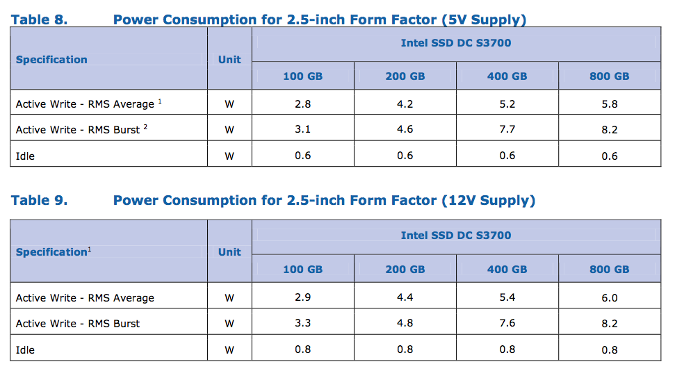
Like previous enterprise drives, the S3700 features on-board capacitors to commit any data in flight on the drive to NAND in the event of a power failure. The S3700 supports operation on either 12V, 5V or both power rails - a first for Intel. Power consumption is rated at up to 6W under active load (peak power consumption can hit 8.2W), which is quite high and will keep the S3700 from being a good fit for a notebook.
Performance & IO Consistency
Performance is much greater than any previous generation Intel enterprise SATA SSD:
| Enterprise SSD Comparison | ||||||
| Intel SSD DC S3700 | Intel SSD 710 | Intel X25-E | Intel SSD 320 | |||
| Capacities | 100 / 200 / 400 / 800GB | 100 / 200 / 300GB | 32 / 64GB | 80 / 120 / 160 / 300 / 600GB | ||
| NAND | 25nm HET MLC | 25nm HET MLC | 50nm SLC | 25nm MLC | ||
| Max Sequential Performance (Reads/Writes) | 500 / 460 MBps | 270 / 210 MBps | 250 / 170 MBps | 270 / 220 MBps | ||
| Max Random Performance (Reads/Writes) | 76K / 36K | 38.5K / 2.7K IOPS | 35K / 3.3K IOPS | 39.5K / 600 IOPS | ||
| Endurance (Max Data Written) | 1.83 - 14.6PB | 500TB - 1.5PB | 1 - 2PB | 5 - 60TB | ||
| Encryption | AES-256 | AES-128 | - | AES-128 | ||
| Power Safe Write Cache | Y | Y | N | Y | ||
Intel is also promising performance consistency with its S3700. At steady state Intel claims the S3700 won't vary its IOPS by more than 10 - 15% for the life of the drive. Most capacities won't see more than a 10% variance in IO latency (or performance) at steady state. Intel has never offered this sort of a guarantee before because its drives would vary quite a bit in terms of IO latency. The chart below shows individual IO latency at steady state (displayed in IOPS to make the graph a bit easier to read) for Intel's SSD 710:
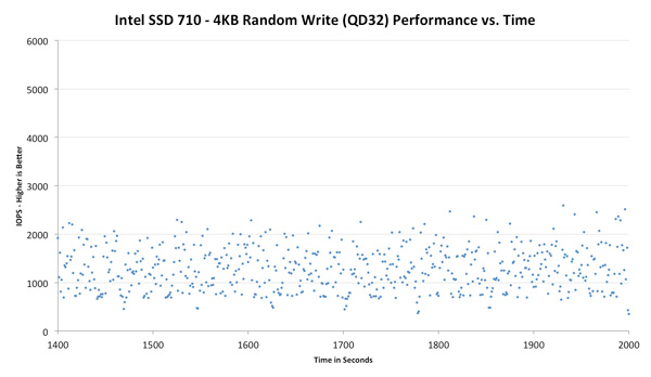
Note the insane distribution of IOs. This isn't just an Intel SSD issue, click the buttons above to look at how Samsung's SSD 840 Pro and the SandForce based 330 do. All of these drives show anywhere from a 2x - 10x gap between worst and best case random write performance over time. Lighter workloads won't look as bad, and having more spare area will help keep performance high, but Intel claims the S3700 is able to tighten its IO latency down to a narrow band of about 10 - 15% variance.
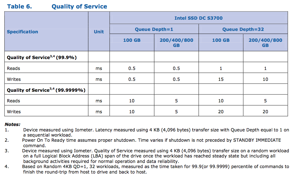
Intel also claims to be able to service 99.9% of all 4KB random IOs (QD1) in less than 500µs:
To understand how the S3700 achieves this controlled IO latency, we need to know a bit more about Intel's older controllers. In researching for this article, I managed to learn more about Intel's first SSD controller than I ever knew before.


43 Comments
View All Comments
DukeN - Monday, November 5, 2012 - link
Now please give us some results with benchmarks relevant to enterprise users (eg RAID performance, wear levelling vs other enterprise drives).chrone - Monday, November 5, 2012 - link
finally getting more consistent performance over time. nice writing Anand, as always! :)edlee - Monday, November 5, 2012 - link
on paper this is very nice, but i am not having any issues with current crop of ssds.how about intel helps design a new sata standard that supports more than 6Gbps, like 50Gbps, so its futureproof, and can put a deathblow to thunderbolt.
Conficio - Monday, November 5, 2012 - link
You realize that* Thunderbolt is an Intel technology. So they are not looking to kill it
* That thunderbolt can rout your entire PCI bus across physical locations (6 m now, with optical cables ~100 m [if memory serves me])
* That said you want SSD interfaces going directly to the PCI bus (not invent another intermediate bus that is built for a technology (spinning disks))
* That direct PCI interfaces for SSDs is where things are going
dananski - Monday, November 5, 2012 - link
"...direct PCI interfaces for SSDs is where things are going"I would like to see this become more common. There's 8Gb/s of spare PCI-E bandwidth on one slot on my machine at the moment.
But what if SSDs advance faster than even PCI-E? I wonder if they could bring the interface even closer to home by allowing NAND chips to plug into memory-like slots on the motherboard (yay easy upgrade path), with the controller integrated into the CPU? The controller should be relatively inobtrusive - how much die area would it take at 22nm? And could some of the operations run efficiently on the main CPU to cut down that die area overhead some more?
JohnWinterburn - Monday, November 5, 2012 - link
As much as fusion IO et al would like it to direct PCI interfaces are certainly not where it's going for this market.You cant replace them easily when they break (as some are always going to when you have enough), you cant fit that many in a box, you have to rely on a single manufacturer and you're then tied into their software.
None of thats going to change any time soon, so PCI interfaced SSDs will be small scale or for specific projects.
ogreslayer - Monday, November 5, 2012 - link
That is what SATA express and SFF-8639 will be for and was announced a while ago.http://www.anandtech.com/show/6294/breaking-the-sa...
Maybe not 50Gbps but at 4GB/s and providing 32Gbps it isn't a small jump. Even the 2Gbps gen3 connection isn't something to sneeze at.
iwod - Monday, November 5, 2012 - link
I still fail to understand why we need SATA express and SFF-8639. When one could have ruled them all. Since the main difference between SATA and SAS is one being Half Duplex and SAS being Full Duplex. But the under lying PCI-Express protocol is Full Duplex by design, so why make another SATA express and not just use SFF-8639 ?And I hope we start with PCI-E 3.0 too, by the time these things arrive there is no point of using the older and slower PCI-E 2.0
Kevin G - Monday, November 5, 2012 - link
Look into SATA-Express. It essentially uses two PCI-E 2.0 lanes for data transfer (16 Gbit/s with 32 Gbit/s when the spec migrates over to PCI-E 3.0). There is some backwards compatibility with SATA too.Though SATA-Express will likely coexist with Thunderbolt. SATA Express is aimed as an internal storage solution where as Thunderbolt is aimed toward external peripherals (where storage is just one aspect).
Kevin G - Monday, November 5, 2012 - link
I'm curious about the raw depth of ECC in this device. ECC on the internal SRAM is pretty much expected for enterprise grade equipment nowadays. ECC on the DRAM is also expected but I'm wondering how it is implemented. Chances are that the drive doesn't house 9 DRAM chips for traditional 72 bit wide ECC protected bus. ECC on the NAND could be implemented at the block level (576 bit blocks with 512 bit data + 64 bit ECC) but that'd require some custom NAND chips.As for the indirect tables, I suspect that the need to be able to hold the entire table in DRAM stems from the idea of table having to optimize the copy in NAND. Optimizing here can likely be done without the massive DRAM cache but I suspect that the optimization process would require too many read/writes to the point it'd be detrimental to the drives life span.