Click Here to Read Even More about the i820 Chipset in our Pentium III B Review
It’s the chipset we’ve all been told to wait for, and it’s finally here, the elusive "Camino" chipset has finally been released as the i820 on this day, the 27th of September in 1999.
Actually, no, it hasn’t. Due to a bug just recently discovered in the chipset, the i820 has been, as you’ve probably already heard, delayed until further notice. This is a huge hit for Intel because this is the first time they’ve truly screwed up a chipset launch. Sure, there have been delays before, but never have they come within a few days of releasing a product and had to cancel the launch due to a severe problem with stability. Could this be the market slipping through their clutches? Is it time for AMD and VIA to step in and take control of the industry?
Let’s not get too dramatic now, because, whether or not that is the case has yet to be determined and the bottom line is that Intel’s 820 has been delayed yet again. Luckily, we’ve been able to put together a comprehensive preview of the chipset to fill you all in on what you can expect from the platform when it does make its release into the market.
While we’ve all recommended waiting until the release of the i820 before pursuing a new system purchase, what you’re most likely to notice is that the "revolutionary" new chipset isn’t as groundbreaking of an introduction as we were hoping it would be.
This preview will concentrate on the i820 chipset itself and the components that go along with it and not the performance of the i820 in comparison to the BX although we will offer some comparative benchmarks between the two platforms. For a performance comparison of the new Pentium III B running on the i820 platform and the old Pentium III on the BX take a look at our Intel Pentium III 533/600B Review which covers both processors that did make it out the door today in spite of the lack of a i820 to accompany them with.
Once Again: The Accelerated Hub Architecture
The i820 chipset is the second Intel chipset to make use of their Accelerated Hub Architecture (AHA), the first being the low-cost i810. For those of you unfamiliar with the i810’s AHA, here is an excerpt from our i810 review:
The key to the success of the Accelerated Hub Architecture is the substitution of individual hub interfaces for the PCI bus in connecting the various parts of your system to your memory/CPU on the motherboard end of things. Take a look at the acronym PCI, Peripheral Component Interconnect, it doesn't really scream "all-purpose-bus" now does it? Intel took what was once a two-chip solution (North/South Bridge) and converted it into a two chip, three-hub solution, the first implementation being the i810 chipset. The three individual hubs are the Graphics and Memory Controller Hub (GMCH), the I/O Controller Hub (ICH) and the Firmware Hub (FWH). The two main hubs, the GMCH and the ICH are connected via an internal bus that offers double the bandwidth of the PCI bus, 266MB/s. This is a definite improvement over the "old" way of doing things and will shortly become the new standard as far as chipsets go, don't expect Intel to return to the classical way of doing things on the motherboard level anytime soon.
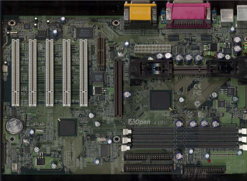
That description of the AHA is pretty much universal and applies almost in every way to the i820. The i820 differs only in its usage of the i82820 Memory Controller Hub (MCH) versus the i82810 Graphics and Memory Controller Hub (GMCH) used in the i810. The reason behind this being that the i820, unlike the 810, does not feature any integrated video, therefore removing the "Graphics" out of the Graphics and Memory Controller Hub and thus shortening it to Memory Controller Hub.


0 Comments
View All Comments