TSMC's 3D Stacked SoIC Packaging Making Quick Progress, Eyeing Ultra-Dense 3μm Pitch In 2027
by Anton Shilov on May 31, 2024 11:00 AM EST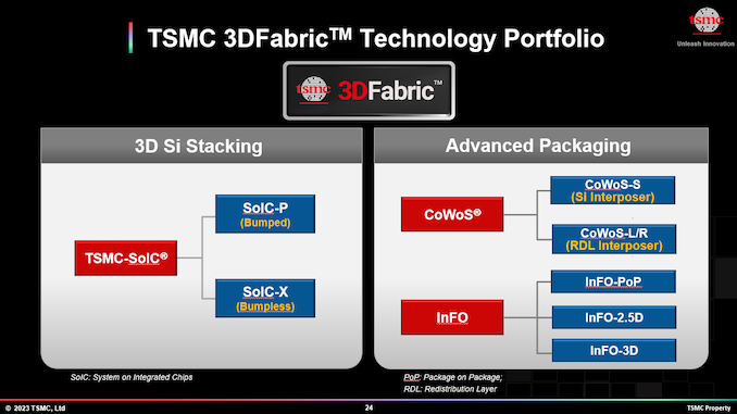
TSMC's 3D-stacked system-on-integrated chips (SoIC) advanced packaging technologies is set to evolve rapidly. In a presentation at the company's recent technology symposium, TSMC outlined a roadmap that will take the technology from a current bump pitch of 9μm all the way down to a 3μm pitch by 2027, stacking together combinations of A16 and N2 dies.
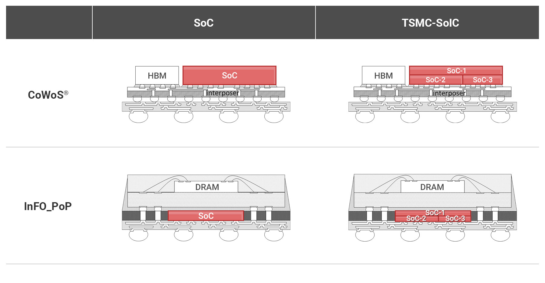
TSMC has a number of advanced packaging technologies, including 2.5D CoWoS and 2.5D/3D InFO. Perhaps the most intriguing (and complex) method is their 3D-stacked system-on-integrated chips (SoIC) technology, which is TSMC's implementation of hybrid wafer bonding. Hybrid bonding allows two advanced logic devices to be stacked directly on top of each other, allowing for ultra-dense (and ultra-short) connections between the two chips, and is primarily aimed at high performance parts. For now, SoIC-X (bumpless) is used for select applications, such as AMD's 3D V-cache technology for CPUs, as well as their Instinct MI300-series AI products. And while adoption is growing, the current generation of the technology is constrained by limitations on die sizes and interconnection pitches.
But those limitations are expected to give way quickly, if all goes according to plan for TSMC. SoIC-X technology is going to advance fast, and by 2027, it will be possible assemble a chip pairing a reticle-sized top die made on TSMC's leading-edge A16 (1.6nm-class) on a bottom die produced using TSMC's N2 (2nm-class). These dies, in turn, would be connected using 3μm bond pitche ssilicon vias (TSVs), three times the density of the size of today's 9μm pitch. Such small interconnections will allow for a much larger number of connections overall, greatly increasing the bandwidth density (and thus performance) of the assembled chip.
| TSMC's SoIC-X Roadmap Data by TSMC (Compiled by AnandTech) |
||||||||
| 2022 | 2023 | 2024 | 2025 | 2026 | 2027 | |||
| Top Die | N7 | N5 | N4 | N3 | N2 | A16 | ||
| Bottom Die | N7 | ≥N6 | ≥N5 | ≥N4 | ≥N3 | ≥N2 | ||
| Bond Pitch | 9 μm | 9 μm | 6 μm | 6 μm | 4.5 μm | 3 μm | ||
| Size* | 0.1 reticle | 0.4 reticle | 0.8 reticle | 1 reticle | 1 reticle | 1 reticle | ||
*TSMC considers reticle size as roughly 830 mm2.
Improved hybrid bonding techniques are intended to allow TSMC's big HPC customers – AMD, Broadcom, Intel, NVIDIA, and the like – to build large, ultra-dense disaggregated processor designs for demanding applications, where distance between the dies is critical, as is the overall floor space used. Meanwhile, for applications where only performance matters, it will be possible to place multiple SoIC-X packages on a CoWoS interposer to get improved performance at a lower power consumption.
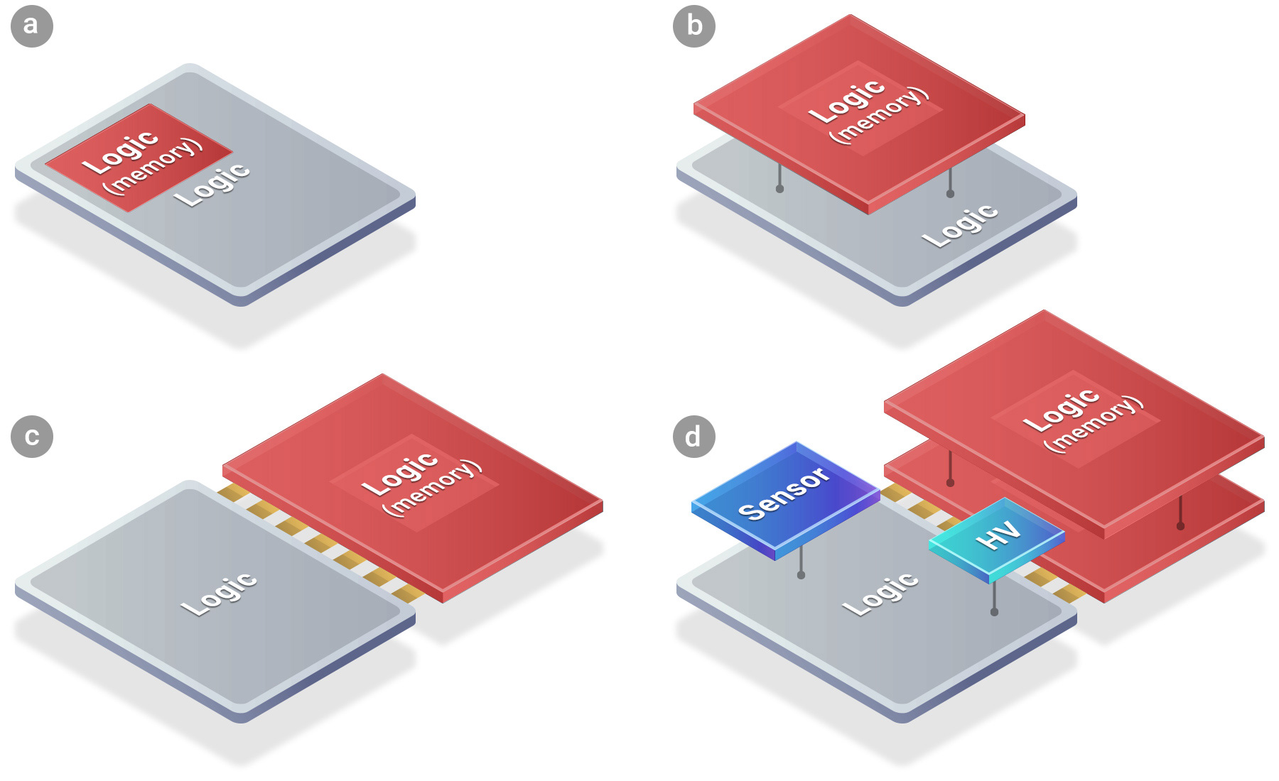
In addition to developing its bumpless SoIC-X packaging technology aimed at devices that require extreme performance, TSMC will also launch its bumped SoIC-P packaging process in the near future. SoIC-P is designed for cheaper lower performance applications that still want 3D-stacking, but don't need the additional performance and complexity that comes with bumpless copper-to-copper TSV connections. This packing technique will enable a broader range of companies to leverage SoIC, and while TSMC can't speak for their customers' plans, a cheaper version of the technology may make it accessible for more cost-conscious consumer applications.
Per TSMC's current plans, by 2025 the company will offer a face-to-back (F2B) bumped SoIC-P technology capable of pairing a 0.2-reticle sized N3 (3nm-class) top die with an N4 (4nm-class) bottom die, which will be connected using 25μm pitch microbumps (µbumps). In 2027, TSMC will introduce bumped face-to-face (F2F) SoIC-P technology, which will be able to place an N2 top die on an N3 bottom die with a pitch of 16μm.
| TSMC's SoIC-P Roadmap Data by TSMC (Compiled by AnandTech) |
||||
| 2025 | 2027 | |||
| Top Die | N3 | N2 | ||
| Bottom Die | ≥N4 | ≥N3 | ||
| Bond Pitch | 25 μm | 16 μm | ||
| Size* | 0.2 reticle | 0.4 reticle | ||
| Die Orientation | face-to-back | face-to-face | ||
| Qualification Time | Q4 2024 for mobile SoC | Q2 2026 for HPC | ||
*TSMC considers reticle size as roughly 830 mm2
A lot of work has to be done to make SoIC more popular and accessible among chip developers, including continuing to iprove their die-to-die interfaces. But TSMC seems to be very optimistic about SoIC adoption by the industry, and expects around 30 SoIC designs to be released by 2026 – 2027.
Source: TSMC Symposium 2024


1 Comments
View All Comments
ballsystemlord - Friday, May 31, 2024 - link
Spelling mistake:"These dies, in turn, would be connected using 3μm bond pitche ssilicon vias (TSVs), three times the density of the size of today's 9μm pitch."
Should read:
"These dies, in turn, would be connected using 3μm bond pitch through-silicon vias (TSVs), three times the density of the size of today's 9μm pitch."