ASML High-NA Development Update: Coming to Fabs in 2024 - 2025
by Anton Shilov on May 26, 2022 10:00 AM EST- Posted in
- Semiconductors
- Intel
- Micron
- SK Hynix
- ASML
- TSMC
- Samsung Foundry
- High-NA
- Intel 18A
It took the semiconductor industry over a decade to prep everything needed for production of chips using extreme ultraviolet (EUV) lithography. It looks like it is going to take a lot less to reach the next level — EUV with High-NA.
Higher Resolution Needed
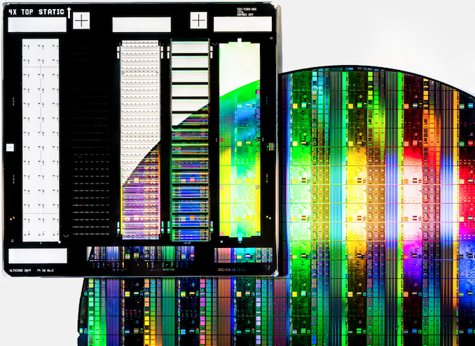
Nowadays the most advanced chips are made on 5/4-nm-class process using EUV lithography ASML's Twinscan NXE:3400C (and similar) systems that feature a 0.33 numerical aperture (NA) optics, which provides a 13 nm resolution. This resolution is good enough for a single-pattern approach at 7 nm/6 nm nodes with 36 nm ~ 38 nm pitches and at 5nm with 30 nm ~ 32 nm pitches. But as pitches get below 30 nm (at beyond 5 nm nodes) the 13 nm resolution might call for dual lithographic exposure that is going to be used for years to come.
For post-3nm nodes, ASML and its partners are working on a brand-new EUV tool — the Twinscan EXE:5000-series — featuring a 0.55 NA (High-NA) lens capable of an 8nm resolution, which is projected to avoid multipatterning at 3 nm and beyond. The new High-NA scanners are still in development, they are expected to be extremely complex, very large, and expensive — each of them will cost over $400 million. High-NA will require not only new optics, but a new light source too, and even new fab buildings to accomodate the larger machines, which will require major investments.
But in a bid to keep scaling performance, power, area, and costs (PPAc) of semiconductors, leading makers of logic chips and memory devices are willing to adopt new technologies, and High-NA EUV scanners are crucially important for post 3-nm nodes. As a result, demand for High-NA tools is, well, pretty high.
10 to 20 High-NA Systems to Be Delivered
Several weeks ago, ASML disclosed that it had received multiple orders in Q1 2022 for its High-NA Twinscan EXE:5200 systems (EUV 0.55 NA) from both logic and DRAM customers. Last week it clarified that it had five orders for pilot High-NA scanners due to be delivered in 2024 and 'over five' orders for subsequent models featuring higher productivity that will be delivered starting from 2025, reports Reuters.
Interestingly, back in 2020 ~ 2021, ASML said that it had has received High-NA commitments from three customers, for a total of up to 12 systems. Keeping in mind that logic makers are usually the first to adopt leading edge tools, it is safe to bet that Intel, Samsung Foundry, and TSMC committed in 2020 ~ 2021 to get pre-production High-NA scanners. Moreover, ASML has already started building the first High-NA system, which will be completed in 2023 and will be used by Imec and ASML customers for research and development purposes.
"On High-NA EUV, we are making good progress and have currently started the integration of the first High-NA system in our new cleanroom in Veldhoven," said Peter Wennink, chief executive of ASML. "We received multiple orders for our EXE:5200 system in Q1. We also received additional EXE:5200 orders this month, April. With these bookings, we now have High-NA orders from three Logic and two Memory customers. The EXE:5200 is ASML's next model High-NA system and will provide the next step for lithography performance and productivity."
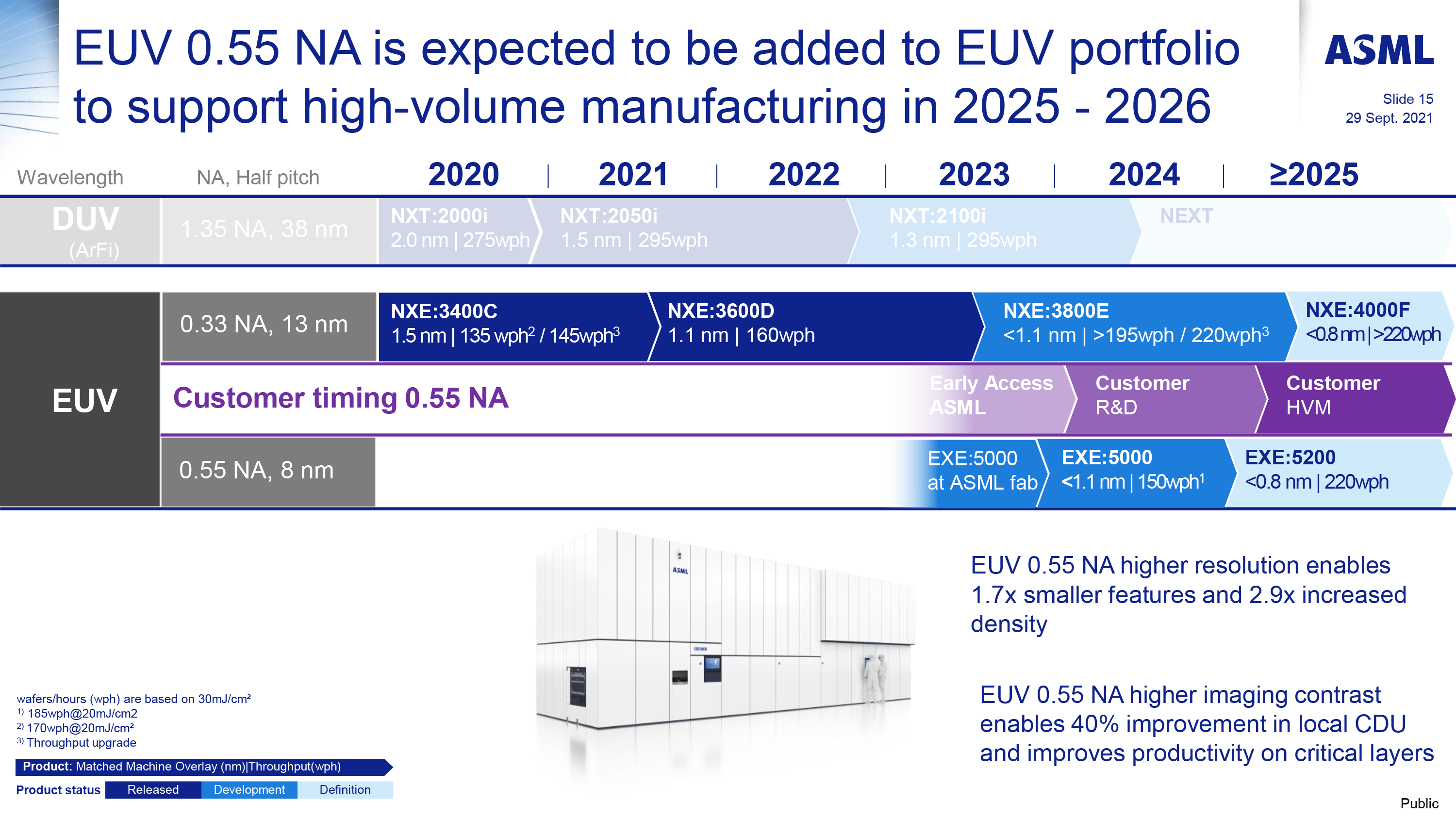
ASML's Twinscan EXE:5200 is considerably more complex than regular Twinscan NXE:3400C machines, so it takes longer time to build these tools. The company hopes that it will be able to deliver as many as 20 High-NA systems in mid-term future, which probably means that its customers will have to compete for these machines.
"We are also discussing with our supply chain partners to secure a capacity of around 20 EUV 0.55NA systems in the medium term," said Wennink.
Intel First to Adopt Pre-Production Tools
So far, the only process technology confirmed to use ASML's High-NA tools is Intel's 18A node and that one was once scheduled to enter high-volume production in 2025, around the time when ASML starts to deliver its production High-NA EUV systems. But recently Intel pulled-in the start of18A production to the second half of 2024 and indicated that it could use ASML's Twinscan NXE:3600D or NXE:3800E for its 18A manufacturing, presumably via multi-patterning.
While Intel's 18A technology would greatly benefit from High-NA EUV tools, it looks like Intel does not necessarily need Twinscan EXE:5200 machines for this node. Usage of multi-patterning for commercial chips means a longer product cycle, lower productivity, higher risks, and potentially lower yields (though the latter is not cast in stone). Yet, it looks like Intel wants its 18A node to arrive as soon as possible, perhaps because it considers it a major tool that will allow it to recapture process technology leadership from TSMC. Consequently, Intel's updated plans are now to phase in High-NA tooling during 18A's lifecycle if the tools are completed on time.
Of course, it remains to be seen whether usage of 0.33 NA EUV scanners for 18A will offer enough productivity for Intel and customers of Intel Foundry Services. But, at least in 2024, Intel is not going to have any choice but to use machines that it has.
Other leading makers of semiconductors — TSMC, Samsung, SK Hynix, and Micron — will also inevitably adopt High-NA EUV for high-volume manufacturing of chips. The only question is when exactly this is when exactly this is set to happen.


7 Comments
View All Comments
edzieba - Thursday, May 26, 2022 - link
Intel have also spent many years pushing DUV very hard, and successfully squeezing water from the multi-patterning stone. That institutional knowledge on how to design processes with the limitations of multi-patterning in mind means they have a good grasp of what is achievable in production and can confidence they can implement it faster than ASML could deliver new units.Arsenica - Thursday, May 26, 2022 - link
Despite being a late adopter of mass-market chiplets products, with the successors of Raptor lake and Ponte Vecchio now Intel is strangely enough better prepared to the halving of the reticle field size consequence of high NA EUV than the companies still pushing for extremely large chips.The halving of the reticle field size means that the maximum chip size will go from 26x33mm to 26x16.5mm and for end products it is the most consequential change that high NA EUV brings, yet AT in the rush of going over PR points not even mentions it in passing.
name99 - Thursday, May 26, 2022 - link
Given the increasing cost and size of all the parts of EUV (not just what's described here, but the other consequences like roughness resulting from stochastic distribution of photons, and the high energy of the electrons released from resist) at what point does it make more sense to switch to direct e-beams for manufacturing?This is a serious question, and the reason I ask is that "we" (ie the Western semiconductor ecosystem) have evolved towards high-NA EUV one step at a time, every step being the obvious short-term maximizer. But have we dug ourselves into a hole? Suppose you were starting from scratch, knowing what's doable via EUV, knowing the costs, but with no existing infrastructure. Would it make sense, instead, to build a direct e-beam based infrastructure?
Given that China (and perhaps Russia, who knows where they will be in five years?) are somewhat in the position I describe (little existing EUV infrastructure, probably little access to such infrastructure, but with the money and smarts to build an alternative e-beam infrastructure --- if that is not completely crazy in terms of the economics...) I think this is an interesting and important question.
My understanding is that ebeam has always been held back by being slower than photon lithography because the beam is not strong enough to flood fill an entire mask area, it needs to be scanned, which slows down throughput. But if the amount of money put into EUV and EUV sources were put into improving the ebeam intensity?... Coupled with if the ebeam equipment took only 1/10th the volume of the EUV equipment?...
Arsenica - Thursday, May 26, 2022 - link
> what point does it make more sense to switch to direct e-beams for manufacturing?At the point that eBeam goes from 1 wafer per day to be able to compete with the 100s of wafers per hour of optical lithography.
Multiple beam eBeam litho is not going to get there any time soon, and anyway it is better suited for extremely repetitive patterns that are not what production of logic chips needs (and memory as a commoditized product is hardly ever on the frontlines of litho development).
back2future - Thursday, May 26, 2022 - link
(in theory) multi-beam lithography might get this into 10's per day for ~10000 beams to 12" wafers (each unit), on ~2012 technology level? (smallest technology target resolution was even ~1nm that time)below 20-30nm it's getting really difficult considering noise because of high energy levels necessary (resulting into constant blur >10nm), secondary electron travel in resist, electron (back)scattering or ensuring data integrity for large areas with (additional) double patterning, what might be necessary for acceptable/improved results or low energy electrons (10-50eV) approach?
"In 2018, a thiol-ene resist was developed that features native reactive surface groups, which allows the direct functionalization of the resist surface with biomolecules."
Anymoore - Sunday, May 29, 2022 - link
As others have mentioned, so many changes come with High-NA EUV, it is still near-revolutionary. It is a different field size, half in fact. This does not match well with older tools in the fab, causing their productivity to drop unnecessarily. The stochastic aspects are also worsened due to targeting smaller spots. It's more likely the secondary electrons will blur out the High-NA resolution. The resists have to be thinner. And, possibly the worst culprit, the optics has obscuration, which was forbiddent in prevous scanner optics designs. High-NA was not supposed to happen when following legal optics designs.kate2030 - Monday, May 30, 2022 - link
very nice..great.https://www.bestreplicawatches.is/