The Qualcomm Snapdragon 855 Pre-Dive: Going Into Detail on 2019's Flagship Android SoC
by Andrei Frumusanu on December 5, 2018 7:00 PM EST
Following today’s early-on coverage of the Day 2 coverage of Qualcomm’s Tech Summit event in Maui, Hawaii, we recap the major story of the day: The new Snapdragon 855 platform. The new platform follows this year’s extremely successful Snapdragon 845 SoC, which we saw power pretty much the vast majority of 2018’s flagship devices.
Qualcomm isn’t standing still, and the Snapdragon 855 represents a new generation, bringing a refresh of the SoC IPs as well a brand new 7nm manufacturing process. Let’s dwell more into today’s details and analyse how the new SoC platform will raise the bar for 2019.
The Finer Details
| Qualcomm Snapdragon Flagship SoCs 2018-2019 | |||
| SoC | Snapdragon 855 | Snapdragon 845 | |
| CPU | 1x Kryo 485 Gold (A76 derivative) @ 2.84GHz 1x512KB pL2 3x Kryo 485 Gold (A76 derivative) @ 2.42GHz 3x256KB pL2 4x Kryo 485 Silver (A55 derivative) @ 1.80GHz 4x128KB pL2 2MB sL3 |
4x Kryo 385 Gold (A75 derivative) @ 2.8GHz 4x256KB pL2 4x Kryo 385 Silver (A55 derivative) @ 1.80GHz 4x128KB pL2 2MB sL3 |
|
| GPU | Adreno 640 @ ?MHz | Adreno 630 @ 710MHz | |
| Memory | 4x 16-bit CH @ 2133MHz LPDDR4x 34.1GB/s 3MB system level cache |
4x 16-bit CH @ 1866MHz LPDDR4x 29.9GB/s 3MB system level cache |
|
| ISP/Camera | Dual 14-bit Spectra 380 ISP 1x 48MP or 2x 22MP |
Dual 14-bit Spectra 280 ISP 1x 32MP or 2x 16MP |
|
| Encode/ Decode |
2160p60 10-bit H.265 HDR10, HDR10+, HLG 720p480 |
2160p60 10-bit H.265 720p480 |
|
| Integrated Modem | Snapdragon X24 LTE (Category 20) DL = 2000Mbps 7x20MHz CA, 256-QAM, 4x4 UL = 316Mbps 3x20MHz CA, 256-QAM |
Snapdragon X20 LTE (Category 18/13) DL = 1200Mbps 5x20MHz CA, 256-QAM, 4x4 UL = 150Mbps 2x20MHz CA, 64-QAM |
|
| Mfc. Process | 7nm (N7) | 10nm LPP | |
At the heart of the new Snapdragon 855 lies Arm’s new Cortex-A76 CPUs: We’ve covered the new microarchitecture extensively this year as we dove into the technical tidbits of the CPU in May, and more recently have been able to deep dive test the performance and power efficiency of the new IP inside HiSilicon’s new Kirin 980. The combination of the new Cortex-A76 with the new 7nm manufacturing node made for great leaps in performance and power efficiency, something that bodes very well for the new Snapdragon 855.
Qualcomm’s take on implementing the new Cortex-A76 cores is quite a bit different than what we’ve seen from HiSilicon. Overall there’s still 4 Cortex A76 derived cores (Kryo 485 Gold as Qualcomm markets them), alongside four Cortex-A55 derived CPUs. The differences here lie in the frequencies, the apparent cache configurations, as well as apparent changes in some microarchitectural tuneables.
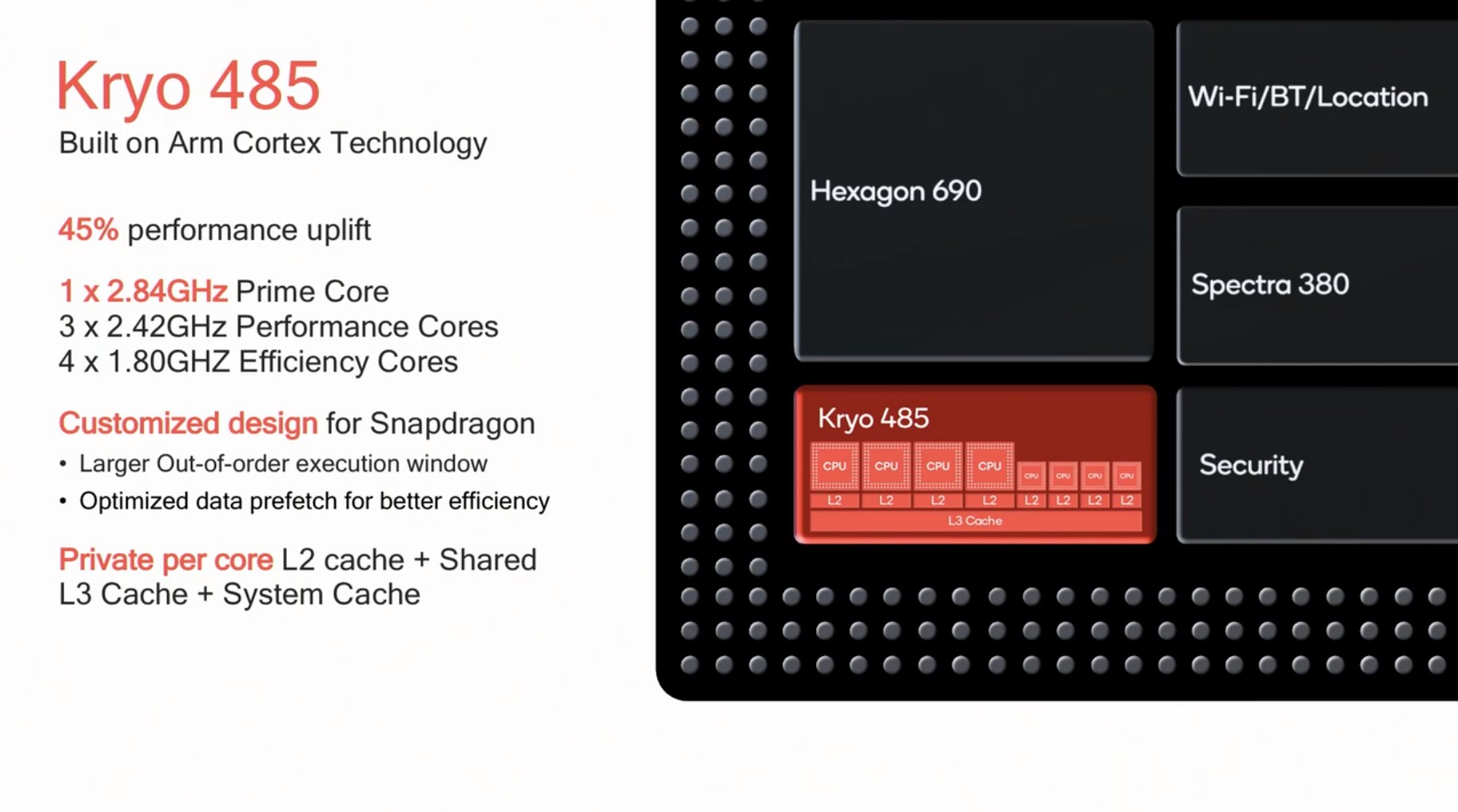
Interestingly, for the first time since Qualcomm has adopted Arm’s “Built on Cortex Technology” license and with the third iteration of its implementation, Qualcomm has finally released details on the kind of changes that have been commissioned to Arm in terms of changes to the IP. Here Qualcomm reveals that the Cortex-A76 variation in the Snapdragon 855 allows for a bigger out-of-order execution window, most likely referring to an increase in the size of the reorder buffer. The stock A76 has a 128 instruction buffer, whereas Qualcomm's modified A76 has been increased to an undisclosed size.
Alongside what seems to be the ROB increase, Qualcomm has also revealed that the data prefetchers have been optimised for better efficiency. It’s not clear if the “efficiency” here refers to power efficiency or the efficiency in the way data is prefetched, nor are the disclosures here what exactly has changes, whether there’s more or less prefetch streams or if there’s been changes in the other types of prefetchers.
While HiSilicon opted for a 2+2 design, where one pair of A76’s were optimised for high frequencies and the second pair were optimised for higher power efficiency, Qualcomm opted to go with a 1+3 configuration.
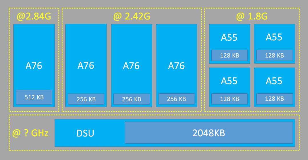
The highest performance core, “Kryo 485 Gold Prime” as Qualcomm calls it, is clocked in at 2.84GHz – putting it on its own clock domain – and is seemingly configured with a 512KB L2 cache. The other three cores are clocked at 2.42GHz and retain smaller 256KB L2 caches. This configuration is quite odd – you also would expect Qualcomm to take advantage of the new DynamIQ cluster design, which is able to support different frequency and voltage planes, however things get even odder. The prime core actually doesn’t have its own voltage plane, and thus it has to share its voltage plane with the other three big cores.
This revelation of the prime core not having its own power domain is quite shocking and it invalidates a lot of the benefits of actually having a separate clock plane for a core. In effect the real-world benefit here isn’t any different than simply clock-gating the core.
It is true that there’s a large amount of scenarios where there’s predominantly a single larger thread active, this is particularly true in web browsing workloads. Such a 1+3 configuration would achieve better performance and possible better efficiency than a 2+2 configuration, but because the cores aren’t running on separate voltage planes it means the actual benefits here in real-world applications are just going to be quite minor. The net result is that the setup is leaving a lot of power efficiency on the table: the voltage supplied to both core groups is always going to be the greater of whatever is being asked for, even if one of the two groups could operate on (much) less voltage.
Qualcomm’s 2.84GHz clock is 9.2% higher than HiSilicon 2.6GHz frequency. A big question here is just how far Qualcomm has driven the core up on the power curve – I am expecting it to be less efficient than the Kirin 980 by some margin, how big that margin will be is something we won’t see until we get our hands on commercial devices.
Most interestingly for today’s presentation is that Qualcomm hadn’t made a single concrete mention about CPU power efficiency of the Snapdragon 855, and I’m not sure if this means there’s no improvements or rather just downplaying this aspect of the SoC given the other significant changes.
Lastly, I do find it odd that Qualcomm went for smaller L2 caches on the remaining 3 high performance cores. I still expect these to end up higher performance than HiSilicon’s 1.92GHz A76 units with 512KB L2’s – but it’s nevertheless interesting to see both companies try to achieve the same goal in different ways.
Moving on, we see the four Cortex-A55 derived efficiency cores, which are running at 1.8GHz and coupled with 128KB L2 caches. In this regard, it seems the Snapdragon 855 doesn’t differ from the Snapdragon 845. Here the company has seemingly put all the process node advantages into improving power efficiency of the little cores.
The DynamiQ Shared Unit’s L3 cache should come in at 4MB – which would be a doubling over the 2MB configuration on the Snapdragon 845. It’s to be noted that we haven’t yet fully confirmed the cache configurations at the time of writing, but I’m strongly leaning towards these figures to be correct. We’ve by now confirmed that the L3 cache has remained at 2MB – this is quite conservative on Qualcomm’s part and there will be an IPC impact compared to the Kirin 980’s 4MB implementation.
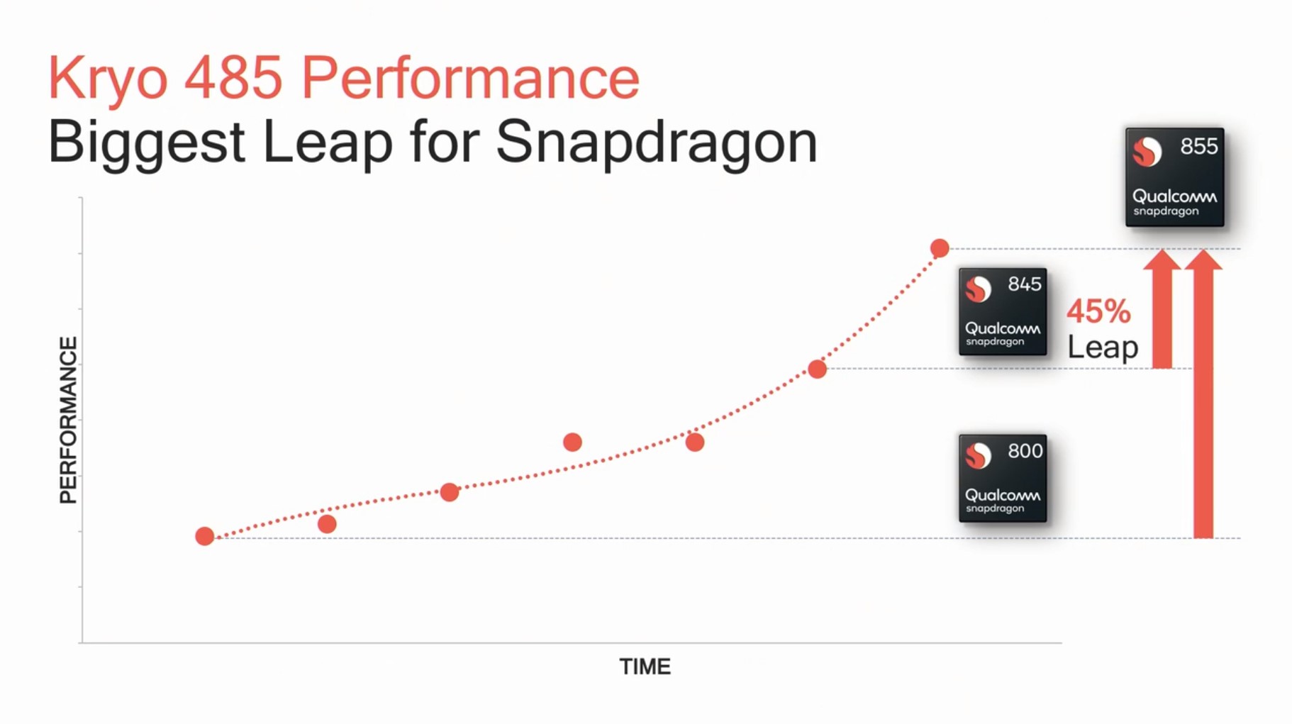
In terms of performance, all that Qualcomm publishes is a claim of up to a 45% performance increase over the Snapdragon 845. As with last year, it’s a bit of a mystery exactly what this figure represents, but the number pretty much falls in line exactly where the Kirin 980 performs in relation to the Snapdragon 845 in SPEC2006. The big question for the S855 is how the new generation system level cache will behave in terms of memory latency, as this will be among the biggest aspects differentiating Qualcomm’s new SoC from its Kirin competition.

Another interesting performance comparison that was published today is a showcase of performance figures between the Snapdragon 855, Apple A12, and the Kirin 980 in terms of app launch times. Though Qualcomm doesn't directly name their competitors, competitors A and B should be the Apple A12 and the Kirin 980 respectively, assuming Qualcomm’s colour scheme is also consistent across the GPU comparisons. For me it’s not to surprising to see the Snpadragon 855 perform this well – one thing I did note in my Huawei Mate 20 review is that the Pixel 3 and OnePlus 6 still felt faster in terms of application launch times. Though this could all just be a side-effect of the scheduler and framework of the Snapdragon chipset rather than the raw CPU performance of the hardware. Of course, software still matters immensely and over the last two years Qualcomm has demonstrated absolute leadership in terms of milking out responsiveness and reactivity out of the hardware through its software designs.
Adreno 640 GPU - Iterative Features and Performance
The Adreno 640 graphics block will be the focus for Qualcomm’s gaming efforts. The company went to great lengths to detail how they felt mobile gaming is on the rise, while other platforms for video games are either stagnating or in decline.

In terms of technical specifications, as is traditional with Qualcomm, we didn’t see much in the way of detailed disclosures on the new GPU. What we did get are more conservative figures, such as a 20% increase in performance. This increase is quite small compared to what we tend to usually see, especially given the fact that the Snapdragon 855 is able to take advantage of a major process node transition.

The Snapdragon 845’s GPU was already the smallest among flagship mobile SoCs at a mere 10.69mm², so unless Qualcomm has significantly increased the number of processing elements inside the GPU cores, this generation should be even smaller. Meanwhile in the event presentation there was one actual titbit about the GPU; Qualcomm is saying that they've increased the number of ALUs for FP32 and FP16 operations by 50%. If my previous estimates about the Adreno 630 were correct, then this would mean the new Adreno 640 sports 384 ALUs per core for a total of 768 ALUs. This ALU increase doesn’t match up with the claimed performance increase, so it’s possible Qualcomm is running the GPU at a lower frequency, or the performance claims were made in regards to possibly less ALU sensitive workloads.
Qualcomm showed a side-by-side comparison between the Snapdragon 845 and the new 855 running PUBG on a cycled script at 40fps. The new chipset was able to showcase a 28% reduction in power on this identical workload. It’s to be noted we don’t really know exactly what point on the power curve this measurement is done, so it’s always a bit of a mystery in terms of direct power comparisons when you do the testing at certain capped performance states.
While the performance gains remain a bit vague at time of writing, Qualcomm did disclose a lot in terms of new graphical features. Here we saw claims that the Adreno 640 graphics in the S855 will enable true HDR gaming, as well games built around Physically Based Rendering. The graphics pipeline will support 10-bit color depth and the Rec 2020 gamut to enable HDR, as well as enabling S855 devices to support the HDR10+ and Dolby Vision formats, which QC states is a world’s first. With the Adreno 640, along with the display IP, devices can support 120fps gaming as well as smooth 8K 360-degree video playback (resolving a major complaint about Snapdragon-power). Just don’t ask how much space those 8K 360-degree videos take up.
Qualcomm's support for Physically Based Rendering in graphics is an interesting topic, one we’ll go into detail in a different article, but the concept is not new. In fact we're a bit surprised to see it mentioned in the same breath as actual hardware changes, since conceptually it shouldn't require any new hardware; PBR is just a shader program that all of the Adreno 600 family should be able to run.
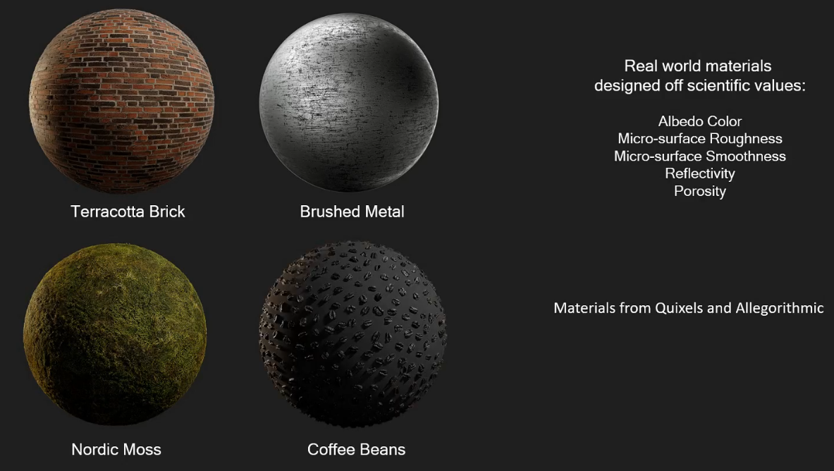
In any case, the short version is that with this enabled, it will help add realism to gaming and augmented reality through more accurate lighting physics and material interactions. Qualcomm stated that through the Unity and Unreal 4 engines, developers will be able to use real world materials designed from scientific values created by companies like Quixels and Allegorithmic that will make their environments more lifelike, such as the correct surface roughness / audio reflections or material-on-material interactions. This will also help with lighting and depth perception. More details to come.


47 Comments
View All Comments
Desierz - Wednesday, December 5, 2018 - link
"one thing I did note in my Huawei Mate 20 review is that the Pixel 3 and OnePlus 3 still felt faster in terms of application launch time"I think it would be better to actually have numbers, rather than what you 'felt'..
III-V - Monday, December 10, 2018 - link
It's a pre-dive. Who cares?Wardrive86 - Wednesday, December 5, 2018 - link
So you estimate 128 ALUs per core/ 256 ALUs total for the A630? I must have read the article wrong because I thought you had estimated 256 ALUs per core /512 total. I was under the impression also that the Adreno 540 was a quad core GPU with 64 ALUs per core/ 256 TotalWardrive86 - Wednesday, December 5, 2018 - link
The 727 Gflop Fmadds you quoted in the earlier article would assume 512 ALUs at 710 mhzAndrei Frumusanu - Thursday, December 6, 2018 - link
I corrected this, it was a brain fart on my part.icalic - Thursday, December 6, 2018 - link
hi Andrei, could you test Adreno 630 on clpeak GFLOPs benchmark and share the result?https://play.google.com/store/apps/details?id=kr.c...
i think 727GFLOPs is too high for Adreno 630 and i believe it only slightly above tegra x1(>512GFLOPs) after i compare score in 3dmark sling shot extreme unlimited graphics. Adreno 630 maybe only have 384 ALU in total.
Andrei Frumusanu - Thursday, December 6, 2018 - link
clPeak isn't accurate.Wardrive86 - Thursday, December 6, 2018 - link
Thank you for the clarificationZolaIII - Thursday, December 6, 2018 - link
A540 is a quad cluster GPU, A630 is dual cluster with 2x more ALU's & it seams A640 is three cluster one on lower clock speed. Also meaning it will have a bit higher mm2 size.Rudde - Monday, December 10, 2018 - link
According to wikipedia (unverified source), adreno 630 has 256 ALUs managing 4x 16-bit FMA calculations per cycle yielding 727 gflops at 710MHz. Assuming adreno 640 is similar, it has 384 ALUs managing 4x 16-bit FMA. 1.2x performance puts it at 872gflops, which suggests a 568MHz frequency.