TechInsights Publishes Apple A12 Die Shot: Our Take
by Andrei Frumusanu on September 25, 2018 11:50 AM EST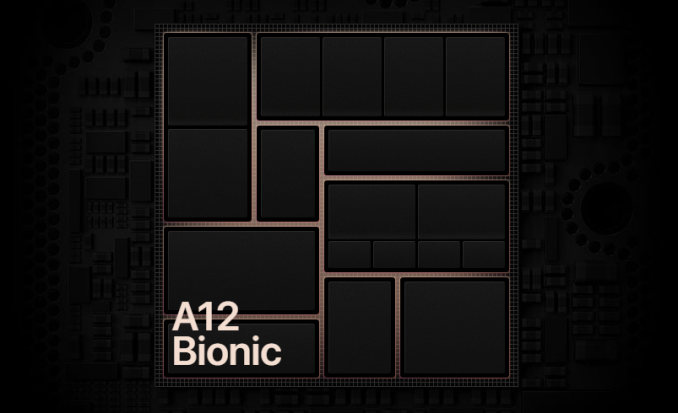
As is custom by now every year, we look forward to TechInsights teardown of the latest new mobile SoCs. This time around we’re delighted to see a new die shot of the new Apple A12, the first commercially available 7nm piece of silicon.
While TechInsights posted their take on the block identification and labelling, found on their iPhone XS teardown blog post, I do think it missed the mark in terms of the CPU complexes. Therefore I did my own analysis and took the liberty of adding a bit more visibility and custom labelling of the die shot:

AnandTech modified TechInsights Apple A12 Die Shot
We see two big cores in the centre-left next to what TechInsights labelled as the NPU. The cores have seen some larger restructuring and this is most obvious in the doubling of the SRAM macros of the L1 data caches which I’ve confirmed to be tested at 128KB – twice the size over last year’s 64KB of the A11 cores. We also similarly see a doubling of the L1 instruction cache macro cells – which also likely hints that this has also seen a doubling to up to 128KB.
The CPU complex cache remains largely the same size as on the A11, with the only difference being a re-layout in a more clean manner. I have big expectations of this part of the new microarchitecture, something we’ll dwell more deeply in our upcoming full review.
The small cores are found in the bottom centre – four of them surrounding their L2 cache logic and memory banks.
The system cache block of the A12 has seen a very major redesign, as opposed to the A11 and prior SoCs, we see a very obvious slice separation into four units. Ironically, at least on the die, this looks a lot more to what we’ve seen in the Snapdragon 845 system cache block.
On the GPU side of things, it’s very clear that this is very much a direct successor to last year’s GPU as the blocks structure in the common shared logic and inside a GPU core is pretty much in line with what we’ve seen last year. We’ll be dwelling into GPU IP discussions more in our upcoming review.
We break down the individual IP block sizes alongside the total die size in the following table:
| Die Block Comparison (mm²) | ||
| SoC Process Node |
Apple A12 TSMC N7 |
Apple A11 TSMC 10FF |
| Total Die | 83.27 | 87.66 |
| Big Core | 2.07 | 2.68 |
| Small Core | 0.43 | 0.53 |
| CPU Complex (incl. cores) | 11.90 | 14.48 |
| GPU | 14.88 | 15.28 |
| GPU Core | 3.23 | 4.43 |
In terms of determining the actual process node shrink, the closest valid apples-to-apples comparison we can make are in the small cores and an individual GPU core. Here we see a shrink from 0.53mm² to 0.43mm² in the small CPU cores – representing a 23% reduction. On the GPU core side we see a more significant 37% reduction down from 4.43mm² to 3.23mm².
All in all Apple is again at the leading edge of manufacturing technology and the new A12 showcases some really interesting changes in its silicon blocks. Stay tuned for our full iPhone XS and XS Max review in the near term future.
Source: TechInsights


34 Comments
View All Comments
Amandtec - Tuesday, September 25, 2018 - link
Remarkable. CPU cores now make less than 3% of the silicon. Who would have thought it...mkozakewich - Tuesday, September 25, 2018 - link
That's each core. Obviously the whole CPU, caches included, are closer to 21% of the die.solipsism - Tuesday, September 25, 2018 - link
You're right, mkozakewich. I just added up the values for the total die size and it didn't even come close to matching, but it works out when you multiply the number of each core type. Too bad they don't like you edit. 🤦♂️Wilco1 - Tuesday, September 25, 2018 - link
The CPUs with L2 are 14%. The system cache is around 6mm^2, so adds another 7%. However the system cache might not be exclusive to the CPUs.Also impressive is 7nm achieved density at 82.9 million transistors/mm^2 - quite close to theoretical density of ~100 mt/mm^2.
tipoo - Tuesday, September 25, 2018 - link
iirc it was part of how they addressed the bandwidth on the phone parts (which have half the memory bit width of the X parts) for the GPU, so the GPU definitely has access.
solipsism - Tuesday, September 25, 2018 - link
My calculations come out to slightly over 3%: 100 * ((2.07 + 0.43) / 83.27) = 3.0022817341%But I don't think that's unusual since this isn't just a CPU, but an SoC with the RAM, GPU, and large CPU complex (which I assume is where the neural engine resides ¯\_(ツ)_/¯).
I wonder how much the 2 cores take up on something like an Apple Watch since that's an SiP.
solipsism - Tuesday, September 25, 2018 - link
Correction: Just the cores are: (((2.07 × 2 big cores) + (0.43 × 4 small cores)) / 83.27) × 100 = 7.0373483848%.Also, it looks like they simply didn't include the neural processing unit in their chart even though I thought the A11 included one last year.
name99 - Tuesday, September 25, 2018 - link
Apple Watch also has GPU and NPU.(The most obvious way to do that would be to assume it gets 1/8 of the A12 NPU complex -- OK, and 1/4 of the GPU complex -- which seems overkill...)
It's still unclear quite how this was handled. Perhaps there's a "natural" way to slice a single Apple GPU core in two?
And of course the two cores on Apple Watch are Tempest cores (the small cores).
DanNeely - Tuesday, September 25, 2018 - link
CPU cores have been a minority of the die area on most consumer facing CPUs for a long time. For complex SoC's this has always been the case because you've got so many not-CPU things packed in. It's also been the case in the PC world since the CPU ate the north bridge and brought the dram controllers and IGPU onboard. GPUless server processors might be an exception, although I wouldn't be surprised if they ended up more cache than compute.dand2 - Tuesday, September 25, 2018 - link
How did you modify the die image colors like that?