Analyzing Falkor’s Microarchitecture: A Deep Dive into Qualcomm’s Centriq 2400 for Windows Server and Linux
by Ian Cutress on August 20, 2017 11:00 AM EST- Posted in
- CPUs
- Qualcomm
- Enterprise
- SoCs
- Enterprise CPUs
- ARMv8
- Centriq
- Centriq 2400
Enterprise Features: Security
With security being a strong focal point in data center tasks, all of the major players that want to provide processors for cloud deployments have been getting their hands dirty and talking security. The ability to provide security keys for hypervisors, VMs, and everything else that can be sandboxed from other users is paramount. To this extent, the Centriq 2400 is supporting two levels of security: EL3 and EL2. This means TrustZone at a system level (EL3) as well as a hypervisor level (EL2), although Qualcomm has not gone into detail if this extends through to having some VMs secure and others not within the same hypervisor environment. Where some of Qualcomm’s competitors are using ARM’s TrustZone implementation – which is an ARM Cortex-A5 for the management – Qualcomm has stated that their solution is not ARM based but a custom design that is TrustZone compliant. We confirmed that this wasn’t another re-use of an ARM architecture license.
Also for security, Qualcomm has added instructions geared towards cryptography acceleration, supporting AES, SHA1, and SHA2-256.
Enterprise Features: Secure Boot
Implementing a Root of Trust has also being making the rounds in recent years. With nefarious code potentially rewriting firmware, or zero-day flaws in technology being exploited by friend and foe, being able to verify the underlying system is as intended and only as intended becomes paramount. Qualcomm’s Centriq 2400 will use Secure Boot functionality.
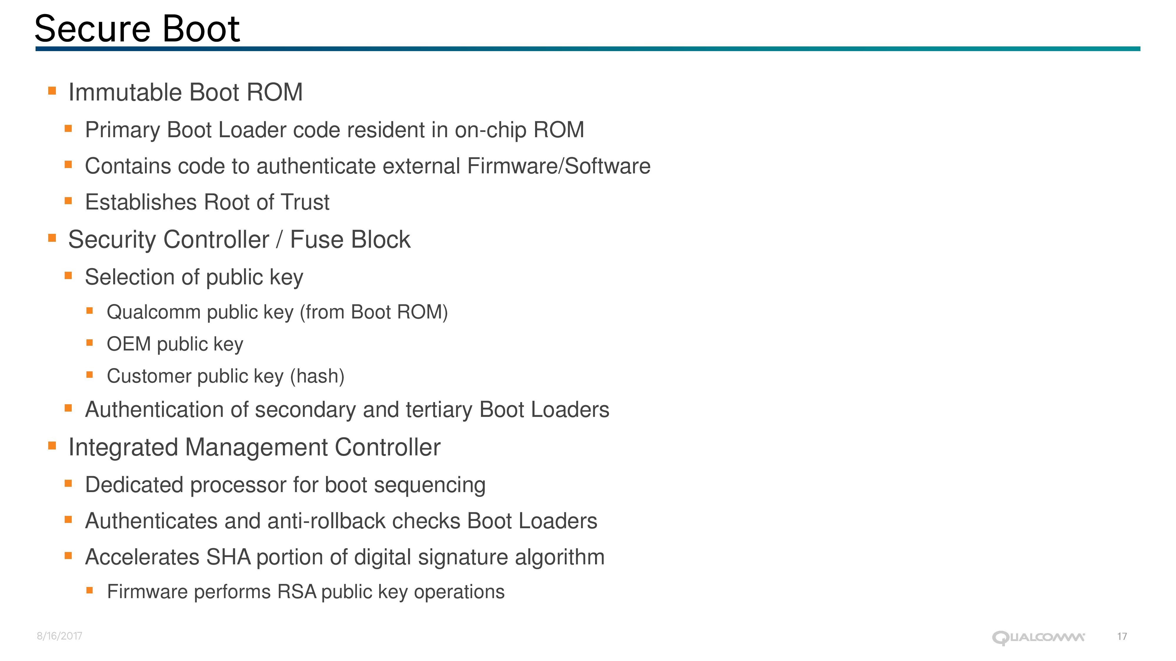
This is accomplished by providing an Immutable Boot ROM via an integrated management controller, with burned in code and cryptographic keys to authenticate firmware and software before any other firmware is loaded. Qualcomm states that this guarantees knowledge of ownership at the base level, as it allows customers to store (at purchase) public keys from Qualcomm, the OEM or the customer to authenticate secondary and tertiary bootloaders with an anti-rollback check. The management controller also supports accelerated cryptography on SHA for digital signatures and RSA public key operations.
Enterprise Features: QoS
Also on the cards is L3 quality of service. In shared resource environments, mission critical applications can be disturbed by ‘noisy neighbors’. With multiple virtual machines vying for the same resources on a single machine, issues such as shared cache contention have flared up in recent quarters for data center use. If one VM is relying on consistent performance from memory accesses from cache but another program is thrashing it and causing inconsistent performance, the user experience can noticeably be disturbed.
There are multiple ways to tackle this, such as increasing the amount of private cache per core/VM, or by providing L3 cache Quality of Service (QoS) features. Intel has done both in recent years, such as increasing the amount of L2 private cache on the Skylake-SP Xeons from 256KB to 1MB, as well as offering L3 QoS since Broadwell-EP. AMD uses 512KB of L2 private cache, and also has QoS in play. Qualcomm isn’t disclosing the amount of L2 or L3 cache in today’s announcement, but were happy to discuss their QoS strategy.
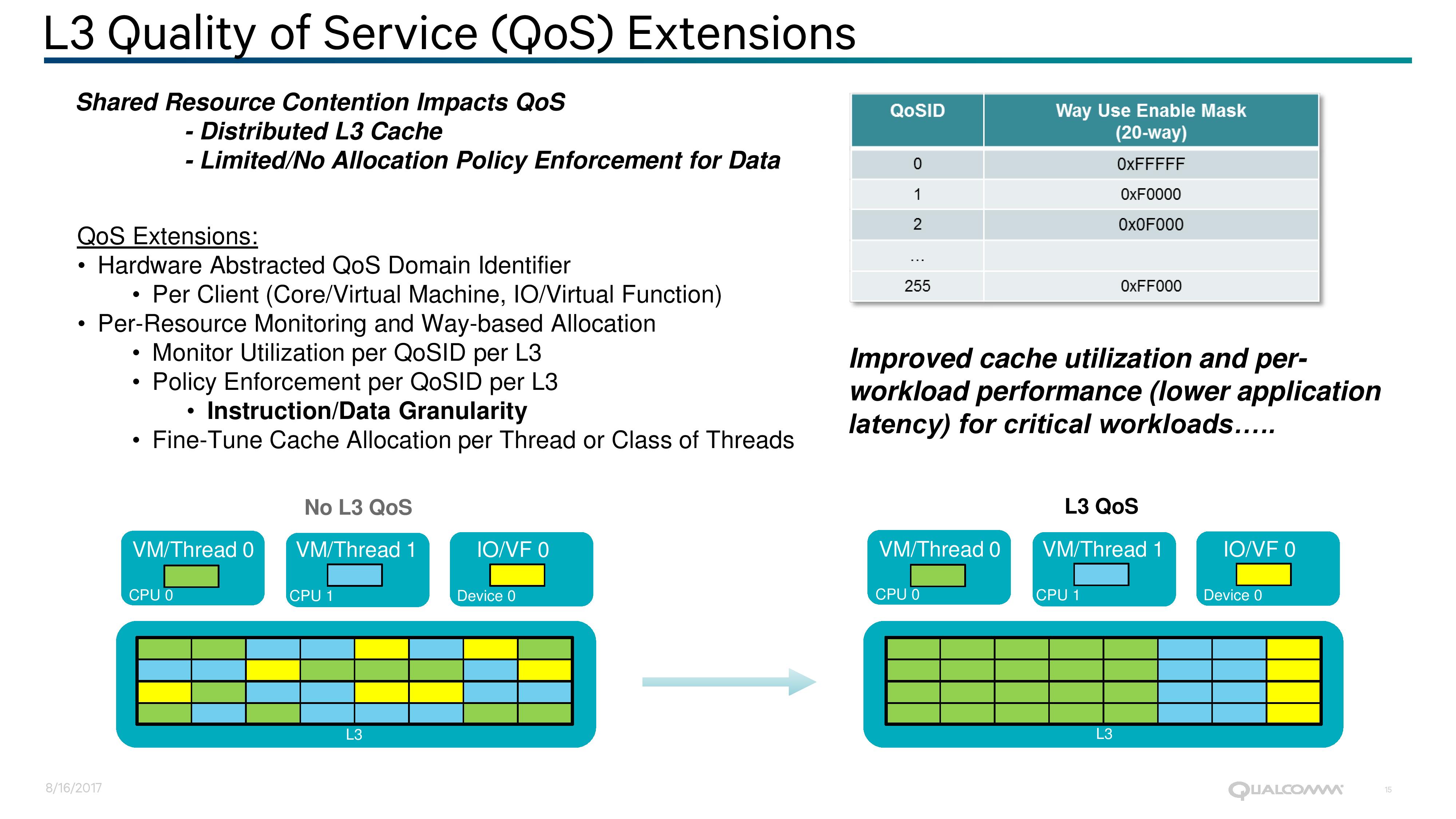
Qualcomm has stated (despite some odd diagrams perhaps suggesting otherwise) that the L3 cache in the Centriq family is a distributed cache, which likely means that each core (or Duplex, more on that later) has a certain amount of associated L3 cache and L3 cache tags with it. By using a hardware abstracted QoS identification method per client, the SoC can monitor resources and enforce L3 QoS policies per domain ID and per L3 segment, down to the instruction and data level granularity. This is done using Way-based allocation, and policies can be adjusted or fine-tuned on the fly per thread or class of threads. Qualcomm’s implementation can support up to 256 defined environments, one of which can be designated or the SoC IO.
Enterprise Features: Memory Bandwidth Compression
One of Qualcomm’s angles in the data center space is going to be that many data center workloads are memory bandwidth constrained. ‘Feeding the Beast’ is the limit for the markets they want to enter, so by enabling transparent memory compression out to DRAM, Qualcomm is attempting to address the issue. This feature will be transparent to any software, with the effect seen mostly in compressible data streams and memory streaming benchmarks.
By using a proprietary algorithm, Qualcomm’s inline compression will attempt to reduce a 128-byte cache line to 64-bytes with ECC as it moves into main memory. When recalling the data back into the core or for committing to storage, decompression adds an additional 2-4 cycles (1-2% on 250-cycle latency) but aims to bring more data in per request than uncompressed data. There could be a slight added benefit of lower power consumption as well, as less data is transferred. We’ve seen these techniques in the GPU space for a number of years.

From the software perspective, the effect will vary considerably from test to test depending on the workload. The Centiq 2400 series comes with six DDR4 memory channels, supporting two DIMMs per channel and up to DDR4-2667, so there’s going to be a lot of bandwidth to begin with – but sometimes that just isn’t enough.


41 Comments
View All Comments
tipoo - Sunday, August 20, 2017 - link
Big ARM server CPUs will be interesting. The ISA is very sane and scalable, if the investment and demand was there it would have no issue getting to where large x86 cores are, the ISA was never the limit.Then we can see if they can actually exceed them.
Kevin G - Sunday, August 20, 2017 - link
This makes me wish that Apple would license their cores to 3rd parties. Recent Apple cores are getting very close to where x86 lies per clock and they've certainly exceeded x86 in performance/watt in the ultra mobile space (granted Intel's last round of ultra mobile chips was flat out cancelled, skewing such a comparison).Considering Apple's work in ultra mobile, I find it believable that a higher performance per clock design in the server space is feasible for an ARM design. A company with enough resources just needs to do it.
iwod - Sunday, August 20, 2017 - link
If the leaked numbers for A11 were true then Apple may have exceeded the performance / clock against Intel x86 as well.While Apple are highly unlikely to ever license their Cores out, I wish they could use those Cores and make an Xserve Server Come back.
peevee - Monday, August 21, 2017 - link
XServe died because of their own OS. Nobody is interested in anything but Linux (and sometimes a little Windows).But they could have sold it with Linux though.
Dr. Swag - Sunday, August 20, 2017 - link
Apple never will though, since it's Apple we're talking about. They keep their tech to themselves to give themselves the advantage.name99 - Sunday, August 20, 2017 - link
The only benchmarks that exist are geekbench4 and the browser benchmarks against Apple laptop hardware. By THOSE benchmarks A9X matched Intel in IPC and A10X exceeds by around 15%.This is clearly an area that draws out the crazies in full screaming mode because a lot of assumptions have to be made (for example the most realistic assumption is that the high-end Intel scores occur at the maximum turbo frequency, but the crazies will insist that, no, you have to normalize to the baseline intel frequency for that particular CPU). Or you get the insistence that the ONLY measurement that matters is against SPEC2006 compiled with icc, which runs into the issues that icc has MASSIVE effects on SPEC; and that no SPEC numbers in any form exist for the A10/A10X.
At the end of the day, it boils down to "what is your goal?" If your goal is an honest comparison of the two processor families, the best data available suggests the summary I gave. If your goal is "my CPU can beat up your CPU" then all the data in the world presumably won't change your mind, and the best data of all is non-existent data (like the certain claims as to how the A10X would or would not behave on SPEC2006).
Final point. It is not at all implausible, IMHO, that Apple have a plan, and have already started proceeding down it, for ARM in their data centers. After all, why not? It saves them money, it allows them to run at their pace not Intel's (eg install AI or compression or encryption accelerators as they need them) and provides better security (both security through obscurity and not having as large an attack surface as Intel).
But why would they talk about it? Apple says nothing ever, unless they have to. No way they would advertise to their competitors the extent to which they have comparative advantage through use of their own data warehouse chips (for at least some purposes).
zodiacfml - Monday, August 21, 2017 - link
Not sa fast. Apple's SoC's are huge in die size which is the reason for their performance. They are as big or bigger than Intel Core. The best part for comparison are the Core M parts. There is little or no business for Apple to do this. There are rumors using Apple SoC on a Macbook Air but that will make little sense as they will to need port OSX to ARM. Again, that is not a good idea as Macbook Pro nor the Mac Pros will continue with OSX .cdillon - Monday, August 21, 2017 - link
Apple has already ported OSX to ARM, and they call it "iOS". It's not going to be as big a deal as you think to get OSX as we know it to run in ARM. Not only that, but they already have experience with juggling two processor architectures (PPC and x86) at the same time in one OS.extide - Monday, August 21, 2017 - link
And 68k to PPC, back in the dayname99 - Monday, August 21, 2017 - link
Apple's SoCs are not huge, neither are their cores.The iPhone SoC's tend to hover around 100 to 120mm^2, the iPad SoCs sometime reach 150, though the A10X is below 100.
The cores are a few mm^2. Eyeballing it, I'd say the entire CPU complex (2 large cores, two small cores, and L2) is about 12mm^2. This is substantially larger than ARM cores (four A73s+their L2 in the same process technology would fit in 8mm^2) but substantially smaller than Intel (an Intel core these days runs at around 8mm^2 in Intels 14nm).