Western Digital Ships Client SSDs Based on 512 Gb 3D TLC NAND Chips
by Anton Shilov on May 19, 2017 3:30 PM ESTLast week Toshiba demonstrated the operation of its XG-series SSDs NVMe PCIe SSD based on the company’s 64-layer 512 Gb 3D NAND chips. What was left unnoticed is that Western Digital made several other important announcements regarding these ICs. First, WD said that it has started to ship both client and datacenter SSDs based on these chips commercially. Second, WD said that the vast majority of 3D NAND flash it produces this year would be 64-layer 3D NAND.
64-Layer 3D NAND Is Here
As reported, both Western Digital and Toshiba started to ship samples of their co-developed 64-layer BiCS 512 Gb 3D TLC NAND chips to their customers earlier this year. The two companies did not formally announce any details about these chips except the most basic ones, so we still do not have any official information regarding the interface speed.
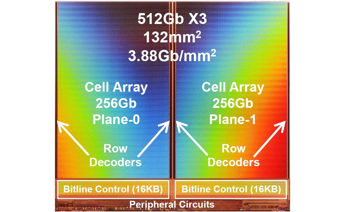
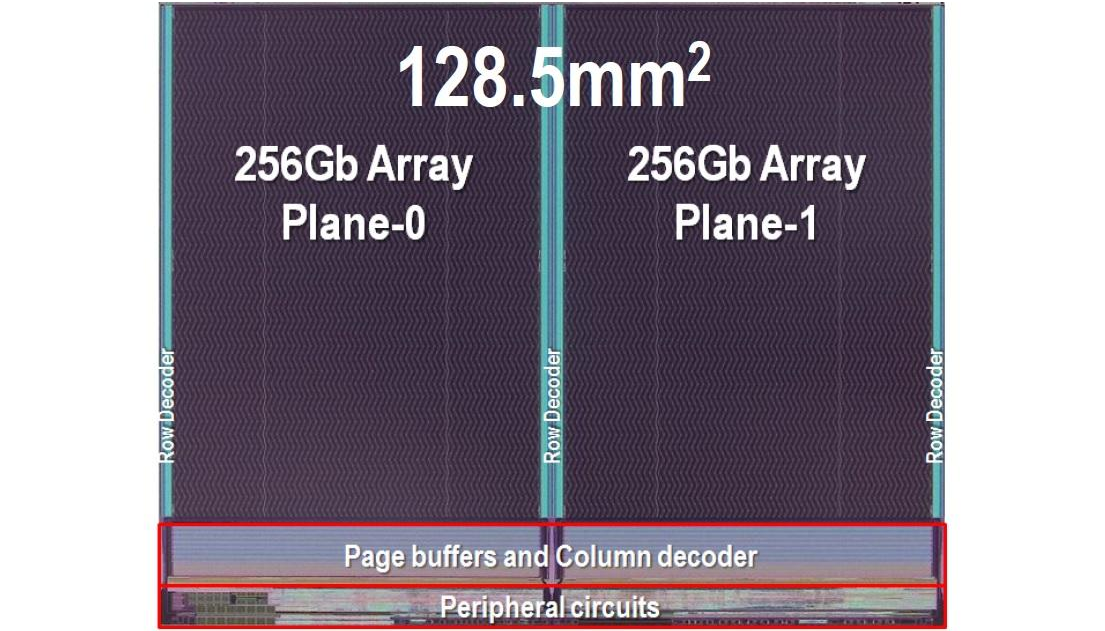
Western Digital’s presentation at the ISSCC reveals that the 512 Gb 3D TLC NAND IC is a dual-plane design with a 132 mm2 die size. From density standpoint, Western Digital’s 512 Gb 3D TLC NAND IC is a little bit behind Samsung’s 64-layer 512 Gb 3D TLC flash chip (which has a die size of 128.5 mm2, according to the company’s presentation at the same conference) that is also a dual-plane IC. Die size and density is one of the important metrics when it comes to the cost of any IC (others are yield, process technology, architecture, etc.) and for many reasons manufacturers do not openly publish it.
Meanwhile, the difference between die sizes of 512 Gb 3D TLC NAND chips from Samsung and Toshiba/Western Digital is so small that it is not going to have a significant impact on costs.
| 3D NAND Die Size Comparison | |||||||||||||
| IMFT | Samsung | WD/Toshiba | |||||||||||
| 1st Gen | 2nd Gen | 1st Gen | 2nd Gen | 3rd Gen | 4th Gen |
1st Gen | 2nd Gen | 3rd Gen | |||||
| Die Capacity | 256 Gb | 384 Gb | 256 Gb | 512 Gb | 128 Gb | 86 Gb |
256 Gb | 512 Gb | 256 Gb | 256 Gb | 512 Gb | ||
| # Layers | 32 | 64 | 24 | 32 | 48 | 64 | 48 | 64 | |||||
| Organization | MLC | TLC | TLC | TLC | MLC | TLC | MLC | TLC | |||||
| Architecture | FG with CMOS under Memory Array | Charge trap flash (CTF) | |||||||||||
| Die Size | 168.2 mm² | 59 mm² | ? | 133 mm² | 84.3 mm² | 99.8 mm² | 128.5 mm² | 105.1 mm² | ~80 mm² | 132 mm² | |||
Die size is only one metric that can indicate the cost of a memory chip. Process, yields and some other peculiarities are other important factors. For example, the ICs have many differences when it comes to their manufacturing method. As reported, the current etching tools cannot “drill holes” in a structure that contains ~60 or ~70 wordline layers simply because it is too thick. Therefore to keep using the current tools, makers need to either make the structure thinner or use two separate structures interconnected using the so-called string stacking technology.
To build their new BiCS 3D TLC NAND chips, Western Digital and Toshiba process two wafers, then stack one above another and connect their NAND strings (enabling NAND controller to see the IC as a single component with a unified address space and manage it appropriately). This requires extremely high precision when placing one wafer atop of each other. In addition, use of the string stacking technology requires Toshiba and Western Digital to process two wafers (with over 32 layers each) to assemble one wafer with 64 active layers of NAND. Keep in mind though that Toshibas has not confirmed string stacking process.
By contrast, to make its 64-layer 3D NAND ICs, Samsung decided to make the structure of its 3D flash memory ICs thinner by making wordline layers (as well as the dielectrics between them) thinner. The move naturally increases the electrical resistance of the wordlines and degrades their retention, which required Samsung to introduce a set of technologies that mitigate the effects of thinner wordlines and dielectrics. The advantage of this approach is that Samsung only has to process one wafer, albeit using a complex process technology.
Western Digital and Toshiba naturally do not disclose costs of their 512 Gb 3D TLC NAND, but WD claims that it has achieved a bit cost crossover for its 64-layer 3D NAND compared to its 128 Gb 2D TLC NAND made using the 15 nm process technology. This means that it is cheaper to build one 512 Gb 3D TLC chip than it is to build four 128 Gb 2D TLC chips, which is not exactly surprising. What is more important is that Western Digital expects 75% of its 3D NAND bits produced this year to use the 64-layer design, which may be an indicator that yields and complexities are in line with its expectations (i.e., string stacking works okay).
WD Ships Client SSDs Featuring 64-Layer 3D NAND ICs
Both Western Digital and Toshiba have been shipping 48-layer and 64-layer 256 Gb 3D NAND chips to their customers for several quarters now. Such ICs are used for removable storage, mobile storage and some other applications. Meanwhile, the 64-layer 512 Gb 3D TLC flash is the first 3D NAND that Western Digital grades for SSDs. Now, a good news is that the company has already started shipments of such drives.
“We commenced shipments of our 64-layer 3D NAND in client SSD form-factor, and we expect to further expand the usage of this industry-leading technology across our product portfolio during the remainder of calendar 2017,” said Michael Cordano, Chief Executive Officer of Western Digital, during an earnings conference call with investors and financial analysts.
Western Digital has not disclosed the controller it uses for its 3D NAND-based SSDs as well as its performance numbers, but since we are talking about initial shipments (presumably to OEMs), we would expect the drive performance to be aimed squarely at OEM customers.
Sources: Western Digital, PCMag, The Memory Guy, TechInsights.


10 Comments
View All Comments
prime2515103 - Friday, May 19, 2017 - link
Western Digital is like a scared little kid that won't leave the school because they're afraid of getting beat up by Samsung. Where is WD's high-end consumer nvme SSD?Gasaraki88 - Friday, May 19, 2017 - link
They don't have a good controller.HomeworldFound - Friday, May 19, 2017 - link
They can't do much until they take over (buy out) more of the market and start fixing prices, that and dragging their heels on increased capacity.prime2515103 - Friday, May 19, 2017 - link
Well I hope they hurry up...edcoolio - Saturday, May 20, 2017 - link
They have a good, but not great, controller.They need to take a company into the fold that can design great controllers. WD can fab them all day if the design is up to par.
In the meantime, they need to keep targeting the low to mid-range consumer market. No choice.
Samus - Saturday, May 20, 2017 - link
I don't understand what happened to the indilinx engineering team behind Barefoot 3 at OCZ. That was one of the most attractive components of that acquisition, imho. After all, who wants the OCZ name?DanNeely - Saturday, May 20, 2017 - link
IIRC part of why Indilinx was an attractive acquisition target at the time was that they were having trouble bringing a new competitive controller to market. I'd guess they've been unable to catch up since acquisition.jjj - Friday, May 19, 2017 - link
What's your source for the string stacking claim?jjj - Friday, May 19, 2017 - link
This press release seems to indicate otherwise, as they brag about high aspect ratio:"IRVINE, Calif., Jul 26, 2016 (BUSINESS WIRE) -- Western Digital Corp. today announced that it has successfully developed its next generation 3D NAND technology, BiCS3, with 64 layers of vertical storage capability. Pilot production of the new technology has commenced in the Yokkaichi, Japan joint venture facilities and initial output is expected later this year. Western Digital expects meaningful commercial volumes of BiCS3 in the first half of calendar 2017.
BiCS3 will feature the use of 3-bits-per-cell technology along with advances in high aspect ratio semiconductor processing to deliver higher capacity, superior performance and reliability at an attractive cost. ""
MIcron and Intel are suspected to be using string stacking( and not confirmed AFAIK) but WD/Tosh, that's a new one.
Anymoore - Wednesday, May 24, 2017 - link
There is a picture of their BICS3 here: http://www.computerworld.com/article/3166187/data-...The bottom part strongly suggest string stacking as the source line (the tall yellow shaft) is not connected to any of the memory pillars at the bottom. They probably extend down to the bottom of the next lower string.