Qualcomm Snapdragon 805 Performance Preview
by Anand Lal Shimpi on May 21, 2014 8:00 PM EST- Posted in
- Tablets
- Snapdragon
- Qualcomm
- Mobile
- SoCs
- Snapdragon 805
Last year Qualcomm announced a new tier in its high end SoC roadmap with the Snapdragon 805. Priced somewhat above the current Snapdragon 800/801, the 805 would be the last 32-bit high-end SoC from Qualcomm. It would be the grand finale in Krait's lineage, which started back in 2012 with Krait 200 and MSM8960 and saw iterative improvements over the years. The Snapdragon 805 was not only designed to drive CPU performance higher but also be the launch vehicle for Qualcomm's brand new Adreno 4xx GPU architecture.
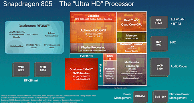
The Snapdragon 805 SoC is a beast. It features four Krait 450 cores, each a mild tweak of the Krait 400 design used in the S800/801. These cores can now run at up to 2.7GHz compared to 2.5GHz in the Snapdragon 801 (Krait 400). As always, Qualcomm advertises customer-friendly frequencies rounded up to the nearest 100MHz, the actual max frequency of each Krait 450 core is 2.65GHz (compared to 2.45GHz in Krait 400).
The 8% increase in max frequency comes from tuning at the circuit level, there's no impact to IPC. All four cores sit behind a shared 2MB L2 cache. As is the case with all multi-core Krait SoCs, each CPU core can be power gated, clock gated and even clocked independently of the rest.
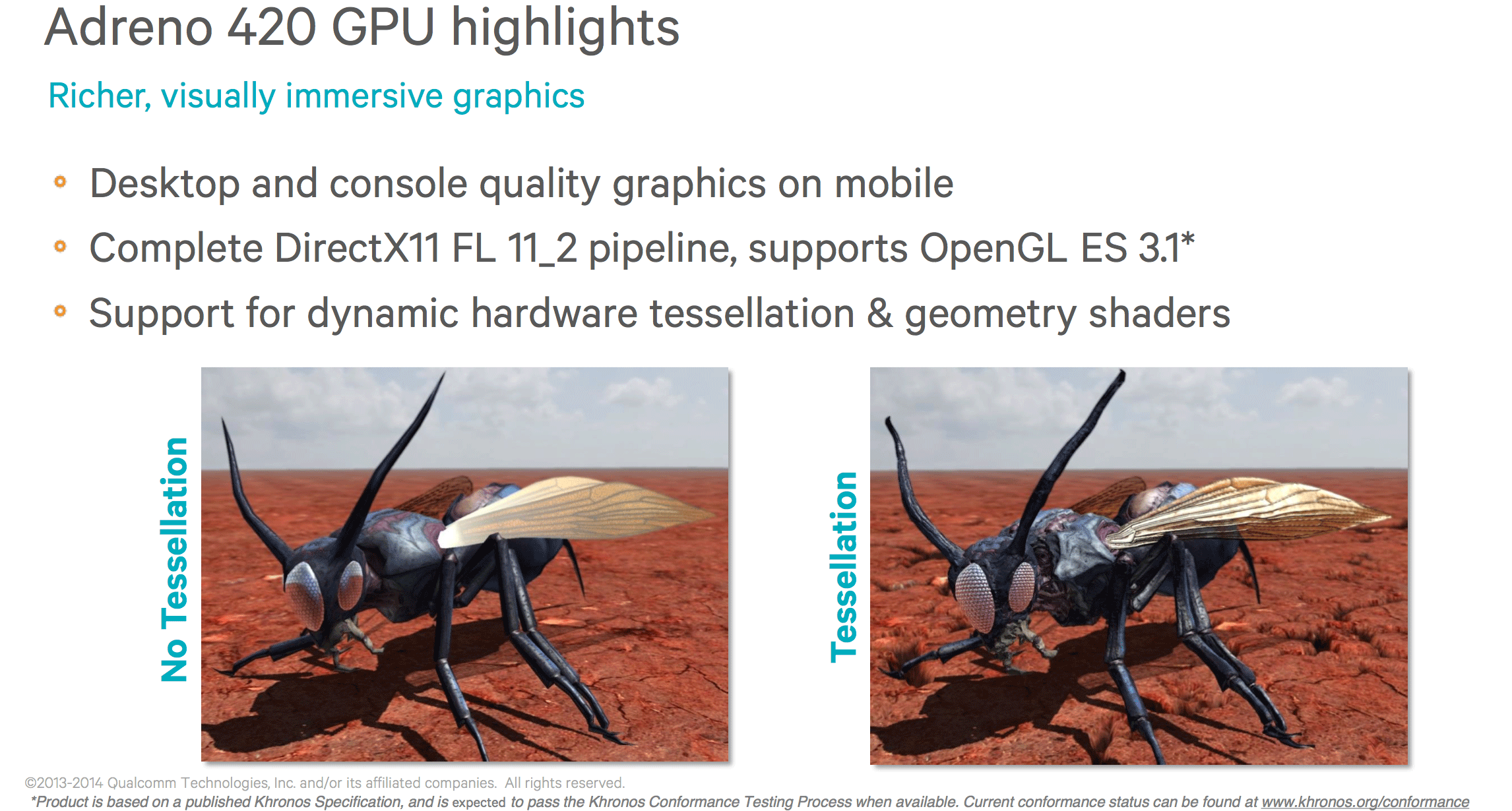

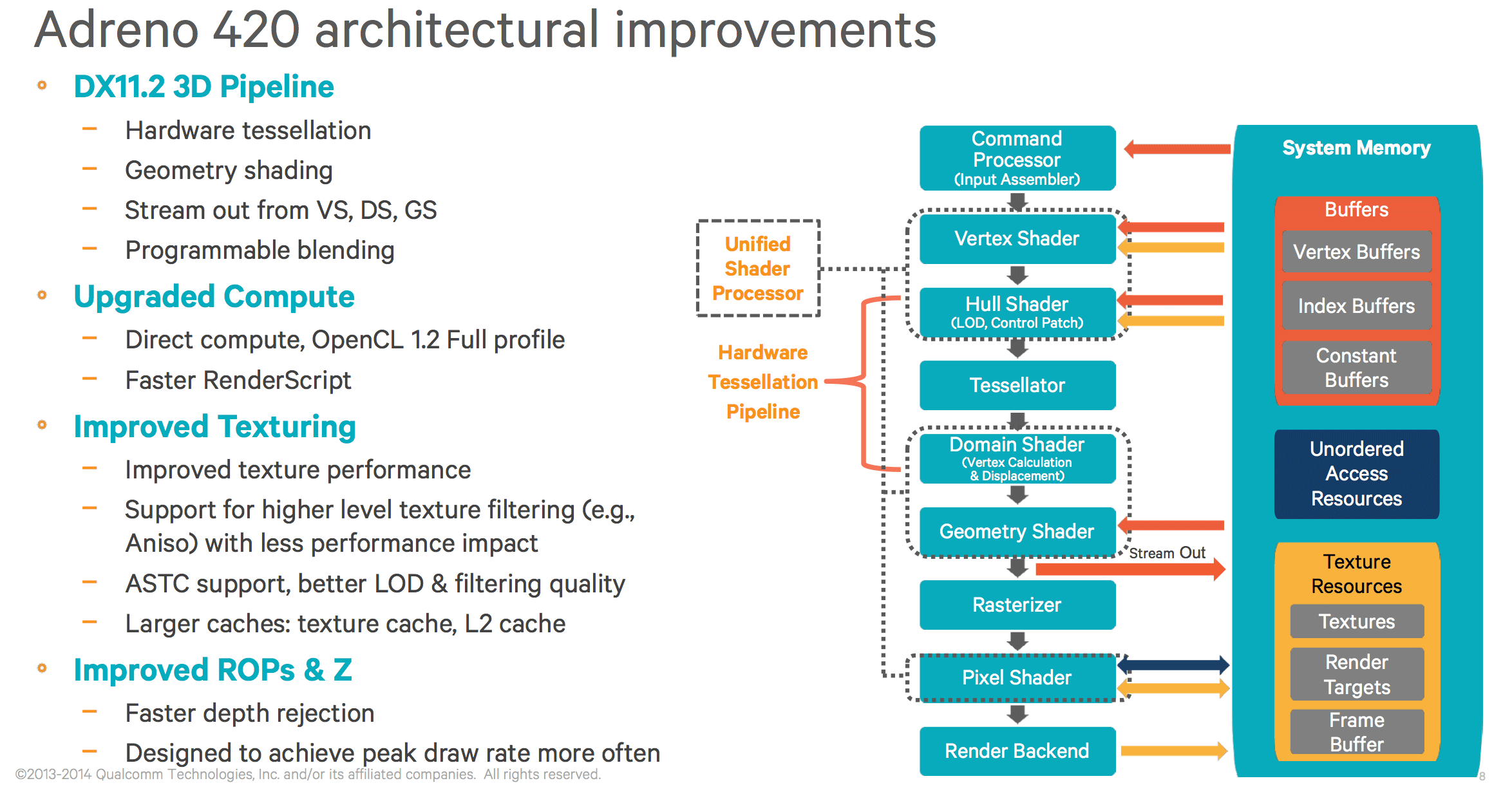
The S805 features Qualcomm's Adreno 420 GPU with full support for OpenGL ES 3.1 (with some extensions), OpenCL 1.2 and Direct3D feature level 11_2 (with a hardware tessellation engine). In typical Qualcomm fashion, it isn't disclosing any material details on the underlying Adreno 420 architecture so we'll have to guess based on what the benchmarks tell us. Adreno 420 includes support for Adaptive Scalable Texture Compression (ASTC), a new texture compression first introduced by ARM in 2011.
There are other architectural improvements including better texturing performance and faster depth rejection. The architecture should be more efficient than Adreno 3xx as well, making better use of the underlying hardware.
The GPU runs at a max frequency of 600MHz.
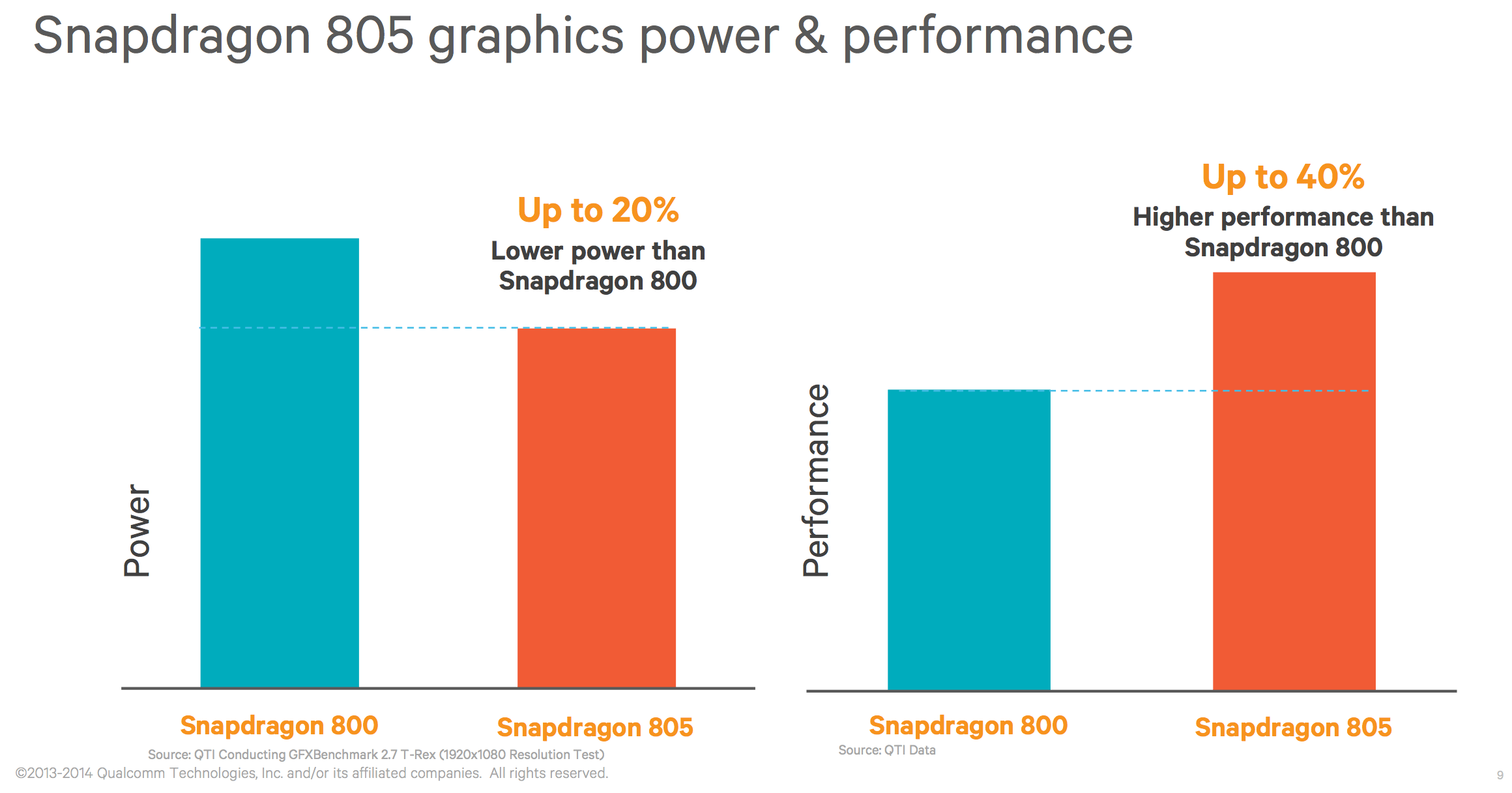
Qualcomm claims a 20% reduction in power consumption compared to Adreno 330 (Snapdragon 800) when running the T-Rex HD test from GFXBench at 1080p (onscreen).
For the first time, the GPU now gets its own direct path to the SoC's memory interface. In the past the GPU shared a bus with the ISP and video engines, but in order to feed the beast that had to change. The memory interface on S805 features two 64-bit LPDDR3-800 partitions (4 x 32-bit external interfaces), each capable of supporting 1600MHz datarate LPDDR3 for an aggregate peak theoretical bandwidth figure of 25.6GB/s. The Krait 450 cores themselves aren't big enough to use all of that memory bandwidth. The wide memory interface is really there for the GPU and video engines. We haven't seen a memory interface this wide on a mobile SoC since Apple's A5X/A6X designs.
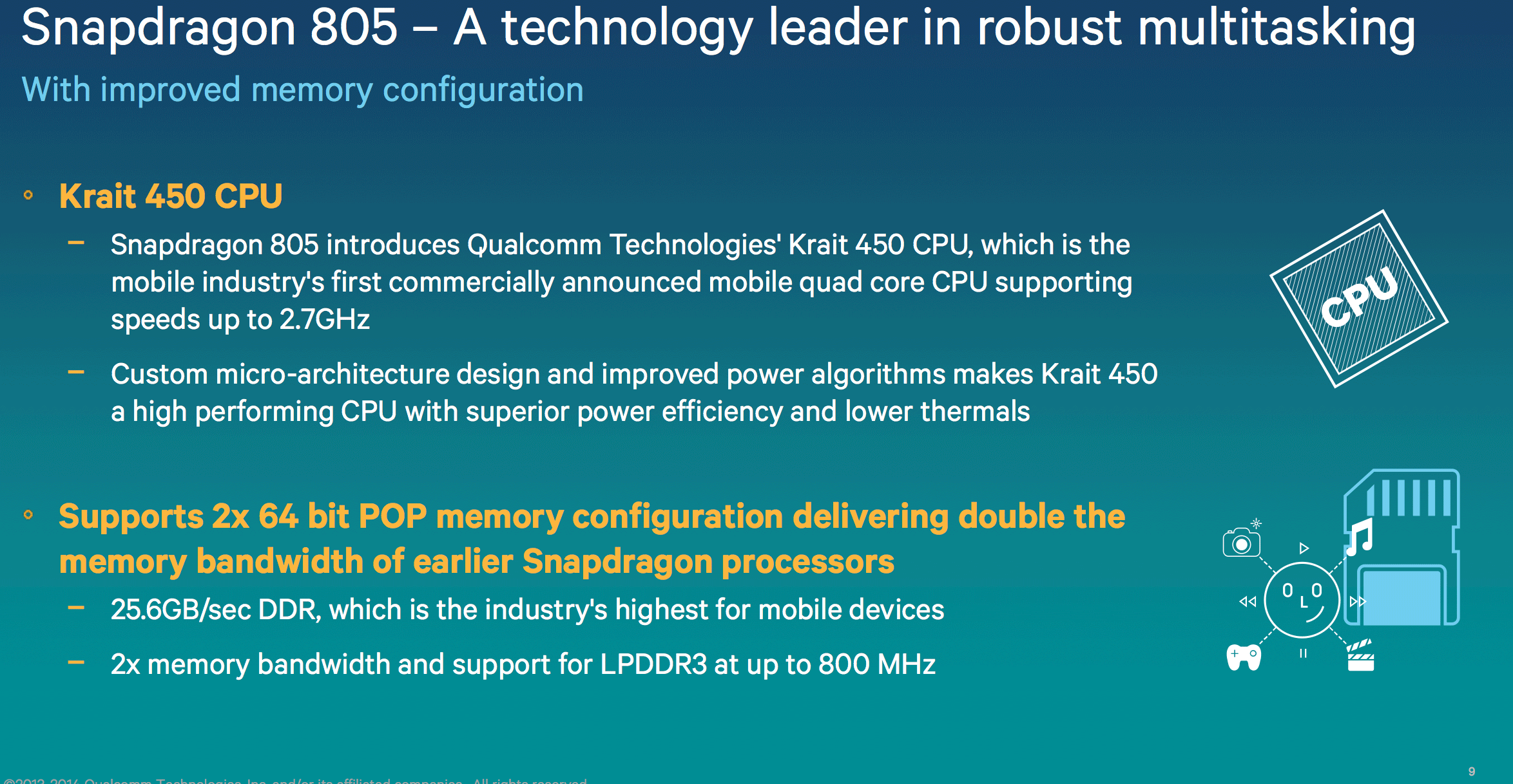
In order to accommodate the wider memory interface but still make Snapdragon 805 suitable for use in a smartphone as well as a tablet, Qualcomm turned to a different packaging technology. Since the Snapdragon 805 is an APQ part, it lacks the integrated modem of the MSM SoCs we've found in most of Qualcomm's recent flagships. S805 uses a Moulded Embedded Package (MEP) that allows Qualcomm to route its 128-bit wide memory interface to on-package DRAM, giving it all of the benefits of a PoP stack as well as the wider memory interface. Qualcomm wouldn't provide me with a ton of details on MEP other than to say that rather than using the perimeter of the SoC's package to connect to memory stacked above it, MEP uses a substrate layer on top of the SoC to connect to the memory, giving the SoC more surface area to route lines to the DRAM. Qualcomm also claims the amount of metal it uses in the DRAM's substrate layer has some small impact on improving thermals on the overall package. The result is that Snapdragon 805 is still compact enough to go into a smartphone as long as the design can accomodate a discrete modem.
The Snapdragon 805 also marks Qualcomm's first SoC with a hardware H.265/HEVC video decode engine. There's no hardware H.265 encode acceleration however, that won't come until Snapdragon 810 in 2015.
The S805's ISP sees an increase in performance as well. The SoC retains Qualcomm's dual-ISP design, now capable of pushing up to 1.2 Gigapixels/s through the engine. If Qualcomm arrives at that number the same way as it has in the past, that would imply a 600MHz ISP operating frequency (up from 465MHz in the Snapdragon 801). The new ISP supports up to four MIPI camera inputs (TrioCam + FF anyone?). The ISP can support 4k30 and 1080p120 video capture.


Qualcomm also claims improved autofocus performance and better noise reduction.
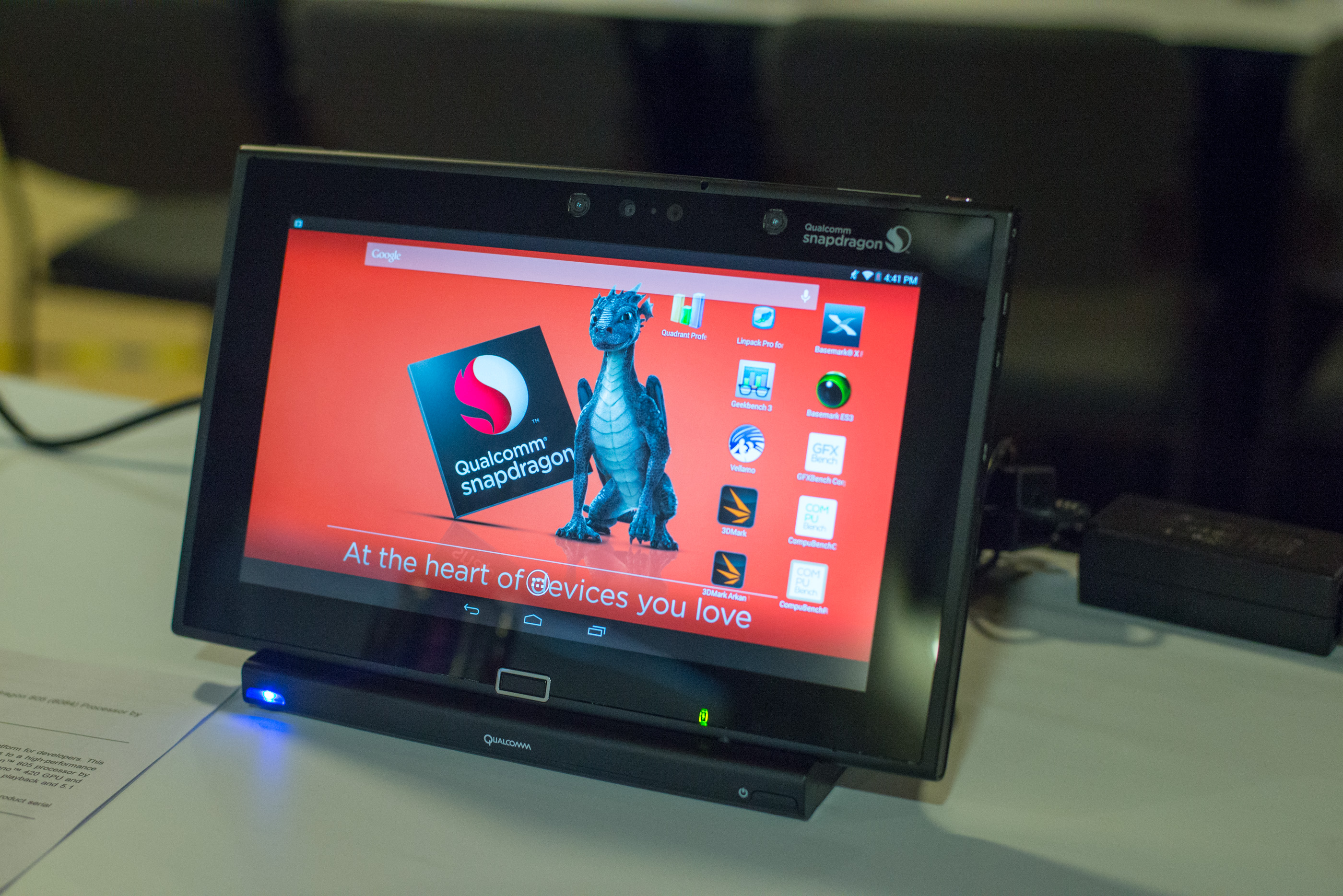
Just as in years past, Qualcomm invited us out to a benchmarking workshop to get some hands on time with its Snapdragon 805 Mobile Development Platform (MDP) ahead of actual device availability. And just like we saw with the Snapdragon 800 benchmarking workshop, the S805's MDP comes in tablet form.the Snapdragon 805 MDP/T features a 10.6" 2560 x 1440 display, 3GB of LPDDR3 memory and 64GB of internal storage (eMMC 5.0). The chassis looks very similar to previous MDP/T designs.
Just as before, the benchmarks that follow are of a pre-production device that isn't shipping hardware. Although Qualcomm has significantly improved the delta we've seen between MDPs and shipping devices, there's always the caveat that performance could be different once we are looking at a shipping device, running on battery power. Although Qualcomm gave us access to the MDP/T, the devices were running on AC power with no power instrumentation connected. Qualcomm's own data shows a reduction in power consumption for Snapdragon 805 vs. 800, but once again we'll have to wait for shipping devices to really understand the impact of the SoC on battery life. What follows is exactly what the title of this piece indicates: a preview of Snapdragon 805 performance. Although Qualcomm pre-loaded the MDP/T with some commonly used benchmarks, we installed our own copies of everything we ran.
| Qualcomm's Snapdragon 8xx Lineup | |||||||
| Snapdragon 810 | Snapdragon 808 | Snapdragon 805 | Snapdragon 801 | Snapdragon 800 | |||
| Internal Model Number | MSM8994 | MSM8992 | APQ8084 | MSM8974 v3 | MSM8974 v2 | ||
| Manufacturing Process | 20nm | 20nm | 28nm HPm | 28nm HPm | 28nm HPm | ||
| CPU | 4 x ARM Cortex A57 + 4 x ARM Cortex A53 (big.LITTLE) | 2 x ARM Cortex A57 + 4 x ARM Cortex A53 (big.LITTLE) | 4 x Qualcomm Krait 450 | 4 x Qualcomm Krait 400 | 4 x Qualcomm Krait 400 | ||
| ISA | 32/64-bit ARMv8-A | 32/64-bit ARMv8-A | 32-bit ARMv7-A | 32-bit ARMv7-A | 32-bit ARMv7-A | ||
| GPU | Adreno 430 | Adreno 418 | Adreno 420 | Adreno 330 | Adreno 330 | ||
| H.265 Decode | Yes | Yes | Yes | No | No | ||
| H.265 Encode | Yes | No | No | No | No | ||
| Memory Interface | 2 x 32-bit LPDDR4-1600 | 2 x 32-bit LPDDR3-933 | 4 x 32-bit LPDDR3-800 | 2 x 32-bit LPDDR3-800/933 | 2 x 32-bit LPDDR3-800/933 | ||
| Integrated Modem | 9x35 core, LTE Category 6/7, DC-HSPA+, DS-DA | 9x35 core, LTE Category 6/7, DC-HSPA+, DS-DA | - | 9x25 core, LTE Category 4, DC-HSPA+, DS-DA | 9x25 core, LTE Category 4, DC-HSPA+, DS-DA | ||
| Integrated WiFi | - | - | - | - | - | ||
| eMMC Interface | 5.0 | 5.0 | 5.0 | 5.0 | 4.5 | ||
| Camera ISP | 14-bit dual-ISP | 12-bit dual-ISP | 1.2 GP/s | 930 MP/s | 640 MP/s | ||
| Shipping in Devices | 1H 2015 | 1H 2015 | 2H 2014 | Now | Now | ||
I pulled comparison results from our new combined Phone/Tablet 2014 category in Bench. The key comparisons here are the iPad Air (for obvious reasons), ASUS' Transformer Pad TF701T (Tegra 4 in a tablet), ASUS' Transformer Book T100 (Intel's Bay Trail in a tablet) and the HTC One (M8)/Samsung Galaxy S 5 (both are Snapdragon 801 devices). With the exception of the Bay Trail based T100, everything else runs iOS or Android.


149 Comments
View All Comments
ArthurG - Thursday, May 22, 2014 - link
What do we care about clock speeds ? is it now a new metric of performance ? Is A7 running at only 1.3Ghz a slow SoC ? Architecture efficiency and final performance results are what we care about.What is important is that TK1 in MiPad destroys all other Android SoC by good margin (60fps T-rex vs 40 on S805) and with good power efficiency.
is it so difficult to admit it for nv haters ?
hahmed330 - Friday, May 23, 2014 - link
If I run my (nexus 7 2013) playing asphalt 8. My battery runs out in 2 hours only on 50% brightness.I can tell you Tegra K1+RAM on TK1 Jetson consumes 6980mW running full tilt at 950mhz for an actively cooled device. Now remember this is a non mobile device for developers.
ArthurG - Wednesday, May 21, 2014 - link
well your post shows big ignorance of the products.1/ Tegra 4 was on 28HPL process when S800/801/805 use 28HPM that provides nearly 30% better transistors. oranges vs apples and big advantage to QC
2/ T4 uses A15r1 that is not very well optimized for power efficiency. TK1 is now with A15r3 that provides better efficiency.
3/ Tegra K1 and S800/801/805 are made on the the same 28HPM process, so it's a fair comparison.
That means that T4 vs S800/S8001 was an easy win for QC due to many disadvantage over T4 design. But TK1 vs S80x shows completely different story with both using same node.
Finally, TK1 benchs are in the Xiaomi MiPad, a 7.9" tablet, no fan here, and it still smokes S805...
testbug00 - Thursday, May 22, 2014 - link
I will believe it when I See them... Also, the amazing "950Mhz" clockspeed of the K1? Guess where it is in the MiPad?In the 600Mhz range. NVidia has to downclock its parts to fit into tablets. Much less phones.
2. Process choice is a manufacturing choice. Nvidia could not get a HPM design? They suffered. Anyhow, Qualcomm will still probably smoke on pref/watt... which, once again, is what is really important in the phone and in most tablets.
3. Krait "450" cores are the same Krait cores from the 800 (a 2013 product) with more clockspeed. A15r3 is a 2014 product. I can throw meaningless garbage into "fair comparisons" also. You compare the SoC as a whole... K1 will end up faster than the 805. I am convinced of it. Will it matter? Not unless you are looking at putting a chip into a miniPC or a laptop... Or, perhaps a mobile-gamecontroller-with-a-screen. :)
Cannot wait for SHIELD 2.
kron123456789 - Thursday, May 22, 2014 - link
Read this:developer.download.nvidia.com/embedded/jetson/TK1/docs/Jetson_platform_brief_May2014.pdf
fivefeet8 - Thursday, May 22, 2014 - link
The MiPad can get the performance numbers they've shown with a GPU clocked at 600 mhz? And that's a bad thing?testbug00 - Thursday, May 22, 2014 - link
Depends on how/when Samsung, Qualcomm, Mediatek, Rockchip, etc. introduce their next generation chips and how fast they are.Apple's will likely beat this on GPU and CPU while using less power... Because, well, Apple has and continues to spend tons of money on optimization. The biggest part is die size... which is a huge advantage Apple has.
kron123456789 - Thursday, May 22, 2014 - link
Apple is using PowerVR GPU. And only GX6650 is comparable with Tegra K1(but it's have about 600-650MHz max frequency, and, because of that, less GFLOPS)testbug00 - Thursday, May 22, 2014 - link
and if the K1 cannot run at full clockspeed in phones/tablets due to setting reasonable clockspeeds or throttling?Or if PowerVR GPU adds more units, or raises Mhz (no reason to do these, as, raising power consumption (Without partial redesign) and these parts are typically "use X power, get as much speed as possible"
Or if Apple happens to license a GPU architecture from a company they are close with, say, PowerVR... ;)
ArthurG - Thursday, May 22, 2014 - link
apple faster ? proof ?All these SoC manufacturers rely on other companies tech to build their GPU. Unlike Nvidia, they can't come up with something new if their IP supplier doesn't have it. And for now, like it or not, no GPU available this year will be more powerful than mobile Kepler. Shallow it, you can't do anything against that.