Intel Discloses Lakefield CPUs Specifications: 64 Execution Units, up to 3.0 GHz, 7 W
by Dr. Ian Cutress on June 10, 2020 11:00 AM EST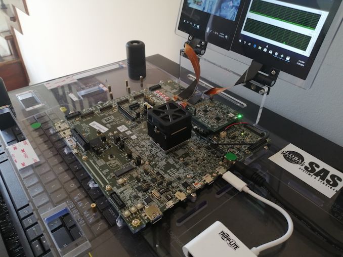
Over the past 12 months, Intel has slowly started to disclose information about its first hybrid x86 platform, Lakefield. This new processor combines one ‘big’ CPU core with four ‘small’ CPU cores, along with a hefty chunk of graphics, with Intel setting out to deliver a new computing form factor. Highlights for this processor include its small footprint, due to new 3D stacking ‘Foveros’ technology, as well as its low standby SoC power, as low as 2.5 mW, which Intel states is 91% lower than previous low power Intel processors. Today’s announcement comes in two parts: first, the specifications.
Intel will debut these two SKUs in its first generation of Lakefield. These CPUs will find homes in premium, always-connected laptops, such as the Samsung Galaxy Book S expected in markets this month, the Lenovo ThinkPad X1 Fold, coming later this year, and in the Microsoft Surface Book Neo.
Both SKUs will feature one big ‘Sunny Cove’ CPU core, along with four little ‘Tremont’ Atom CPU cores. Both sets of cores will have access to a 4 MB last level cache, although Intel has not yet disclosed what sort of cache this is.
Meanwhile on the graphics front, Intel is integrating a Gen11 GPU with 64 execution units, the same number of EUs as on Intel's Ice Lake processors. Interestingly, the iGPU is clocked about half as high as usual for an Intel GPU, with clockspeeds peaking at just 500 MHz – suggesting that Intel is going wide and slow to increase graphics performance. Both CPUs will be rated for a TDP of 7 W.
| Intel Lakefield Processors | ||||||||
| AnandTech | Cores | Base Freq |
1C Turbo |
nT Turbo |
Gen11 IGP |
IGP Freq |
DRAM LP4 |
TDP |
| i5-L16G7 | 1+4 | 1400 | 3000 | 1800 | 64 EUs | 500 | 4267 | 7 W |
| i3-L13G4 | 1+4 | 800 | 2800 | 1300 | 48 EUs | 500 | 4267 | 7 W |
Intel confirmed to us that the base frequency is the unified frequency across all five cores, and the single core turbo frequency applies only to the big Sunny Cove core. Support for LPDDR4X-4266 is a notch above the memory controller in Ice Lake, which only runs at LPDDR4X-3733, and the memory speed will likely be a big boost to performance.

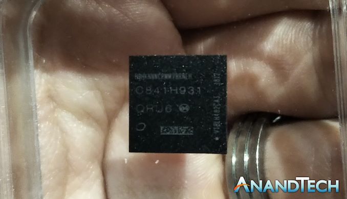
In order to enable these processors in a small 12mm x 12mm footprint, Intel is using its 3D stacking technology, called Foveros. This means that the logic areas of the chip, such as the cores and the graphics, sit on a 10+ nm die, while the IO parts of the chip are on a 22nm silicon die, and they are stacked together. In order to make the connections work, Intel has enabled 50 micron connection pads between the two silicon halves, along with power-focused TSVs (through silicon vias) in order to power the cores on the top layer.
Intel lists the TDP for these chips at 7 W, although the company has not disclosed the turbo power limits for the chip. As mentioned above, Intel hasn’t disclosed how the cache works. In the initial diagrams, we were shown that PoP memory would be added on top, and while Intel hasn't offered further details there, we know from last month's Samsung Galaxy Book S reveal that there will be (at least) 8GB SKUs using LPDDR4X.
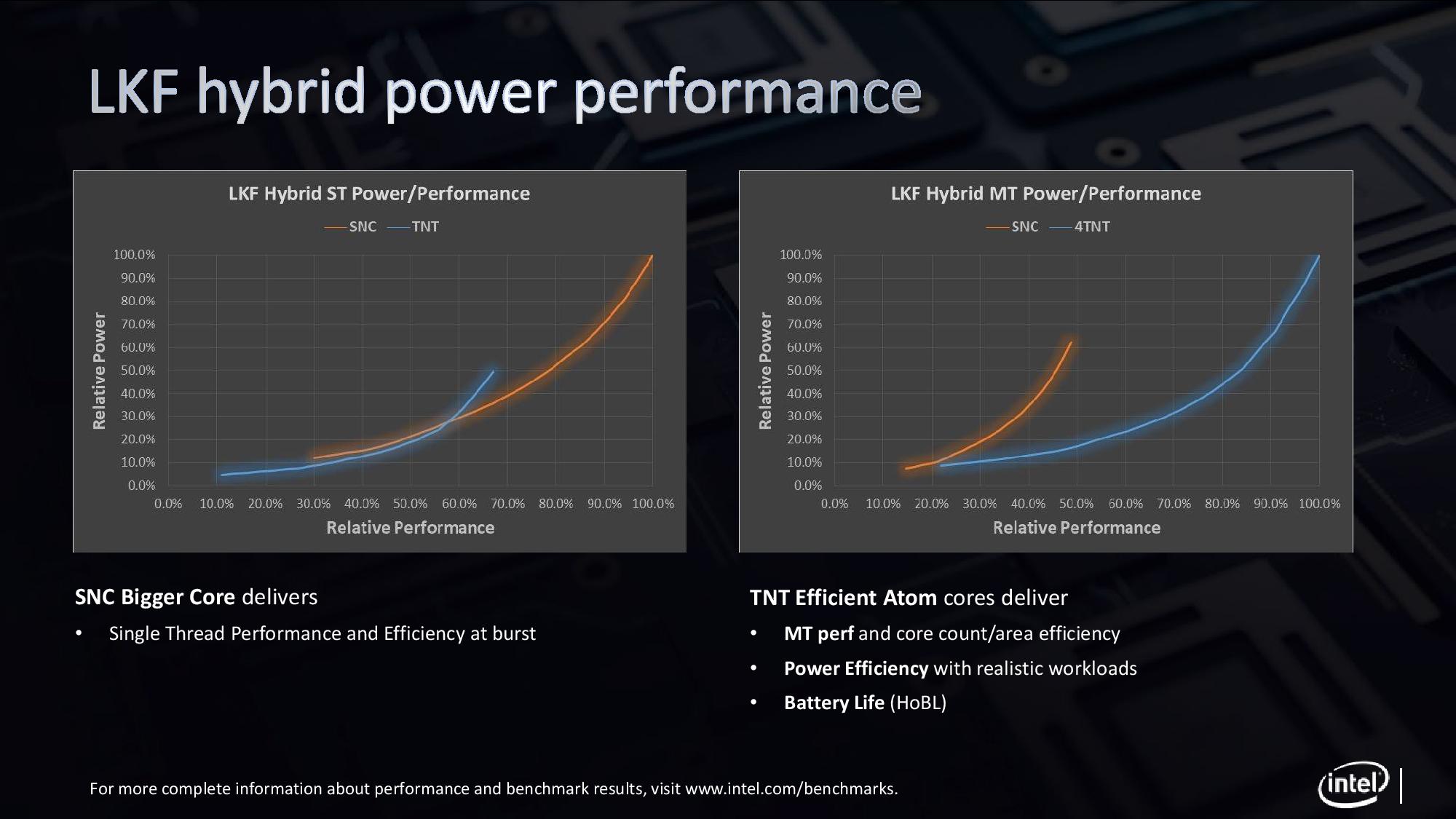
We have big questions as to how each of the cores will work, given that by default they support different instruction sets – Intel hasn’t provided information on this at this time. Intel has stated that the scheduling of the threads on the different parts of the CPU will occur based on hardware-guided OS scheduling, although again Intel hasn’t gone into the details of its hardware tracking and enablement on how this is done. In the demos we have seen, Lakefield will use the Tremont cores for almost everything, and only call on the Sunny Cove core for user-experience type of interactions, such as typing or interacting with the screen.
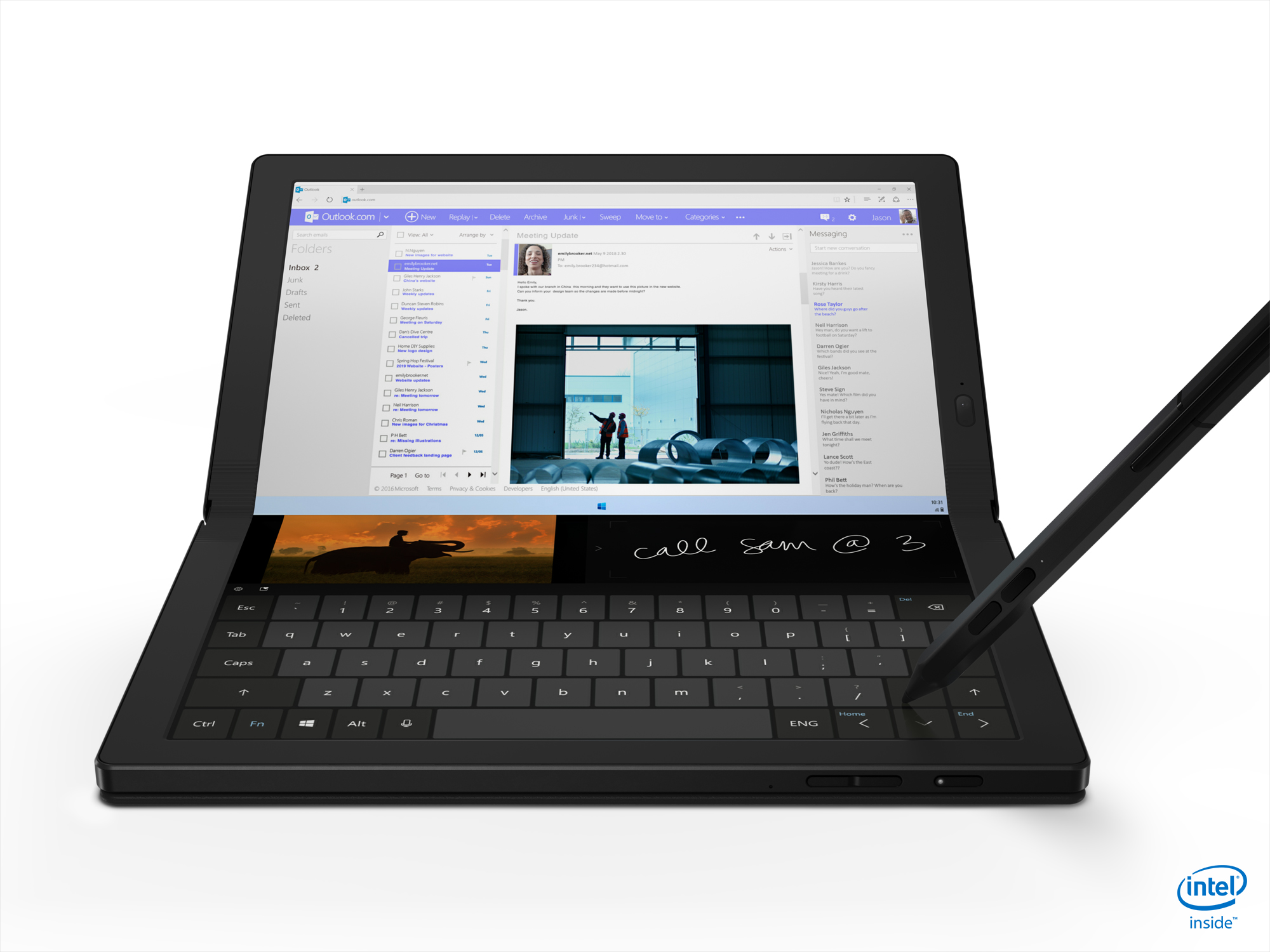
Lenovo ThinkPad X1 Fold
Intel is planning a post-announcement briefing for press to ask questions, which means that this announcement is coming in two parts. This is the information we’re being given beforehand, and we will update you with the details from the post-announcement briefing. As part of this process, we’ve exclaimed to Intel how this way around of presenting details to the press is frustrating – firstly for readers, as you all will have to come back if you want to find out what more Intel tells us later today, but secondly for us, as press, who will have to scramble to jump on the details and decide whether to write fast and miss details, or write slow and miss the wave of traffic.
One thing we can confirm in advance – the Sunny Cove does not appear to be AVX-512 enabled. Intel’s initial press release states that AI workloads occur on the CPU; given the extra power draw required for AVX-512, this is probably a good thing.
More information out of Intel’s post-announcement press-briefing will come later today.


78 Comments
View All Comments
jruhe - Thursday, June 11, 2020 - link
Might be due to the need of an uniform instructions set over all cores.dontlistentome - Thursday, June 11, 2020 - link
Is the TDP 7 real watts or 7 intel TDP watts (~89w in real life)?Deicidium369 - Friday, June 12, 2020 - link
An example of giving people without a clue information they are unable to process. OK - you got your little "joke" in - now run along.Spunjji - Tuesday, June 16, 2020 - link
Intel watts are like dog years :DIn seriousness, though, I'd be surprised if this thing could draw much over 12W even if it wanted to. The Sunny Cove core probably maxes out around 3W at its 3Ghz boost limit, and the Tremont cores are likely to be around half that; that leaves 3 or 4W for the heavily underclocked GPU.
Fr@nk - Thursday, June 11, 2020 - link
Wonder how this first-gen Foveros Lakefield stands up against an ARM Qualcomm 8cx on x86 workload? Qualcomm 8cx cannot emulate x64 apps, only 32 bits x86 apps, right?Samsung has the Qualcomm 8cx on the Galaxy Book S and ditched it for the Lakefield for the next Book S. Comparing both would be great!
eastcoast_pete - Thursday, June 11, 2020 - link
I really look forward to the first reviews of one of these! As much as Intel has screwed up in recent years with the seemingly endless wait for their 10 nm process to become mainstream, this design is really innovative! So, now the wait begins to see if they got the cooling right and the transition from 4 little to one big core snappy enough to make a difference.Assuming all that works out, one question I'd have is if these SoC designs positively exclude adding memory outside the packaging. Something tells me that having Intel package the RAM right in there means that 8 GB will cost ya, and 16 GB might not even be in the cards.
shelbystripes - Saturday, June 13, 2020 - link
This is one of those cases where Intel’s segmentation drives me batty. They’re only targeting this at mobile device makers—but it sounds absolutely ideal for a SOHO/SMB NAS. It could potentially boost the performance of existing x86 NAS in that range (which use Atom-based Celeron/Pentium, aka “little” cores only) without substantially increasing system power. I’m sure there are tasks (disk scrubbing, RAID rebuild, docker instanced, etc.) that would run faster with the “big” core, but you’d still be running most of the core NAS OS on the little cores, and a GPU for Plex HW acceleration.But Intel probably isn’t making it convenient for those vendors to get at all.
Spunjji - Tuesday, June 16, 2020 - link
I suspect you'll see more activity on that front later. Right now they have a very specific target for this: "always connected" mobile devices. In the likelihood that market fails to live up to expectations, they'll need somewhere to shuffle these off to. The tiny boards this can live on could make for a really compact NAS with staggeringly low idle power.