ASML’s First Multi-Beam Inspection Tool for 5nm
by Dr. Ian Cutress on June 1, 2020 10:00 AM EST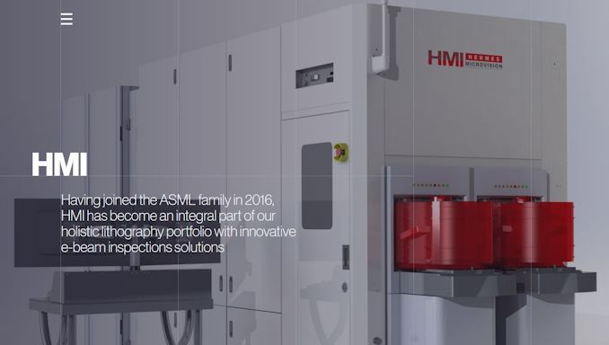
One of the important aspects about developing, designing, and building a new processor in a fabrication plant is the metrology: the analysis of the manufacturing steps throughout the process to ensure that what you want to happen is actually what’s happening. Metrology allows the fabrication plant to identify if machines are working properly, and also help in the characterization of the end product with regards to appropriate voltage/frequency or binning through disabling silicon. If a wafer is particularly bad, it can be discarded earlier in the cycle, therefore saving money and time.
As with many other steps in the fabrication process, metrology is both time and space intensive inside a fab. As with the goal of better lithography machines moving to EUV to both enable smaller features but also speed up processing time per chip, the two main aims of metrology is accurate reporting but also throughput. Increased throughput for these machines means that fewer machines are needed for any given run, and the latency between process node steps can be shortened.
![]()
ASML has announced it has made a significant development in its multi-beam inspectional tool line. The new eScan1000 moves a single beam scanning process into a nine-beam scanning process, which ASML claims increases the throughput of such tools by up to 600% for in-line defect inspection applications. This tool is suitable for all major process nodes in current production as well as 5nm and beyond.
The company explains that the new eScan1000 tool contains an electron optics system that splits a primary beam into multiple beamlets, while also collecting and processing the results from these secondary beamlets. The tool has limited crosstalk to sub-2% to maintain imaging quality, and uses a high-speed mode to increase the overall throughput, and new computational hardware acceleration to process the data from the beamlets quicker than before. The tool is also available at a range of beam currents, assigning it for both physical defect inspection and voltage contrast inspection. ASML promotes the fact that it has a proprietary database that excels in defect detection capabilities, spotting defects missed by more traditional metrology methods.
According to the news, ASML has shipped its first eScan1000 system to a specific customer in Silicon Valley in the past week for initial testing and qualification at a customer site. It isn’t stated who the customer is.
ASML expects to expand its range of eScan1000 machines in order to meet specific customer needs, and says it will continue to develop multi-beam technology with more beams and a wider range of beam resolutions. Given the significance of this tool, we might expect to see a roadmap at a future industry event at some point later this year.
Related Reading
- ASML Ramps Up EUV Scanners Production: 35 in 2020, Up to 50 in 2021
- EUV Demand is Up: EUV Device Manufacturer ASML Beats Sales Estimates
- ASML to Ship 30 EUV Scanners in 2019: Faster EUV Tools Coming
- ASML Ships Twinscan NXT:2000i Scanner for 7nm and 5nm DUV
- Early TSMC 5nm Test Chip Yields 80%, HVM Coming in H1 2020
- EUV Wafers Processed and TwinScan Machine Uptime: A Quick Look
- Intel’s Manufacturing Roadmap from 2019 to 2029: Back Porting, 7nm, 5nm, 3nm, 2nm, and 1.4 nm


19 Comments
View All Comments
bagamut - Tuesday, June 2, 2020 - link
Is he Dr. at all? )FreckledTrout - Tuesday, June 2, 2020 - link
Come on. You guys bagging a tech writer for grammer are just silly.Entropyq3 - Tuesday, June 2, 2020 - link
Yes, but in chemistry. (*snicker*)Actually, so am I, and if you are a computational chemist, you .... burn cycles. A lot of them.
I’m a bit surprised that he chooses to refer to his title when active in another domain, but each to his own. He’s for real though, I actually looked up some of his chemistry work when he started doing this. It’s not for the faint of heart. ;-)
Sherlock - Tuesday, June 2, 2020 - link
I am hoping the ribbing is good natured - He has addressed the topic of including his title before - based on guidance from others in the professionEntropyq3 - Wednesday, June 3, 2020 - link
Well I stepped in to defend his honour. :-)I don’t make the same decision though. My computational chemistry background means little outside of its own context.
rabidpeach - Wednesday, June 24, 2020 - link
plz, do you as phd doctor also confuse is/are when you are writing professionally and get money for doing so?CiccioB - Wednesday, June 3, 2020 - link
<quote>According to the news, ASML has shipped its first eScan1000 system to a specific customer in Silicon Valley in the past week for initial testing and qualification at a customer site. It isn’t stated who the customer is.</quote>How many companies that posses silicon foundries are based in Silicon Valley?
Mmmm.... difficult answer
Sivar - Wednesday, June 3, 2020 - link
Intermolecular Inc. and Integrated Device Technology are the only ones I know of. Even Intel closed their last Silicon Valley fab long ago.FullmetalTitan - Friday, June 5, 2020 - link
I also wondered this. It may not be at a foundry facility. AMAT is also located in San Jose, I could see their interest in validating this platform seeing as how they build the cutting edge tools used in plasma etch platforms and other processes in semicon manufacturing.