Qualcomm Announces Snapdragon 865 and 765(G): 5G For All in 2020, All The Details
by Andrei Frumusanu on December 4, 2019 1:50 PM EST- Posted in
- Mobile
- Qualcomm
- Smartphones
- SoCs
- 7nm
- 5G
- Snapdragon 865
- Snapdragon 765
Immense AI, Camera and ISP Upgrades
New Hexagon 695 DSP: 4x Performance On New Tensor Cores - 15 TOPs Total on SoC
The Snapdragon 865 now ships with the new Hexagon 695 DSP block. The single biggest improvement of the new design is a massive quadrupling of the processing power of the dedicated tensor cores. This jump alone is able to double the SoC’s aggregate AI processing ability up from 7 TOPs to 15 TOPs.
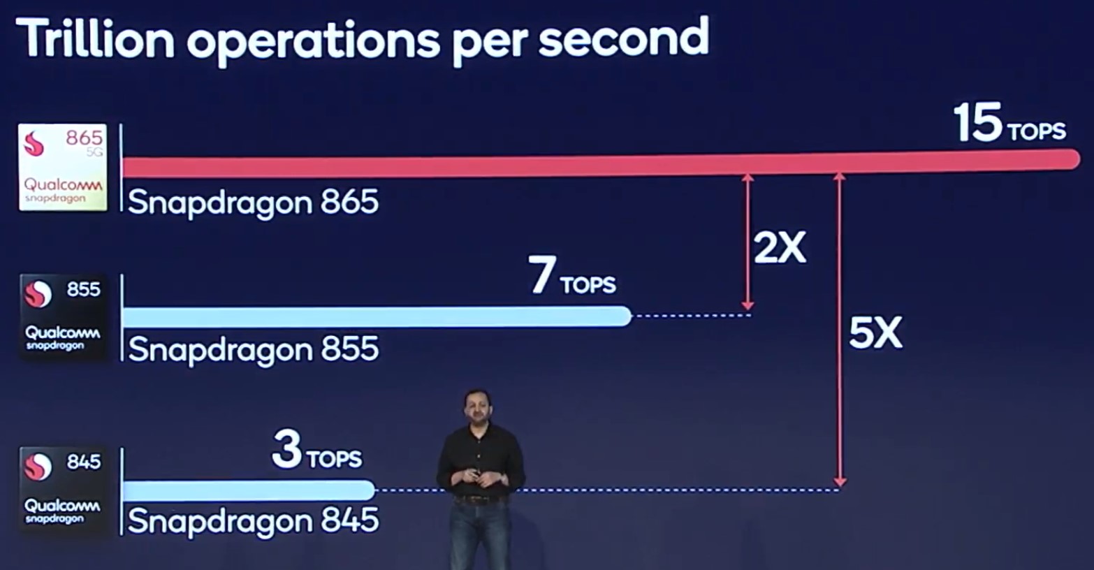
Qualcomm here still doesn’t properly do a breakdown between the IP blocks which contribute to this number, but given that the GPU only saw a ~20% increase, and that the Hexagon’s scalar and vector execution units this year have remained the same in terms of performance, we estimate that the tensor units now roughly come in at around 10TOPs by themselves.
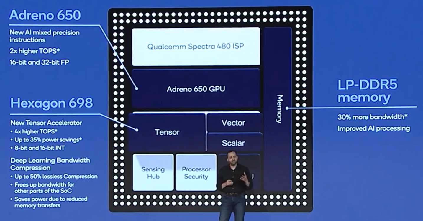
Qualcomm has also now included lossless weight and activation compression for the Tensor cores, being able to reduce bandwidth consumption up to 50%. This is a similar feature we've seen advertised by third-party NPU IP offerings, only that Qualcomm is going to be shipping this now in a product in just a few months.
Power efficiency of the block is also have said to have improved by 35%, making computations less costly in terms of battery life.
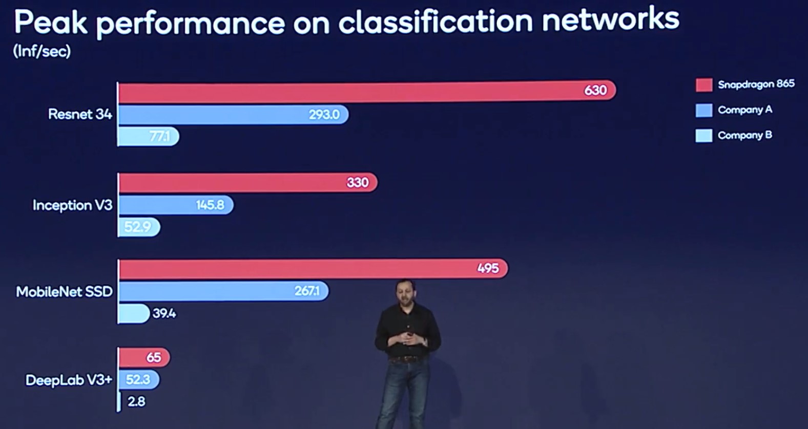
Qualcomm talks how about its inference performance and inference power efficiency is significantly higher than competing solutions. We don't know the comparison SoCs being showcased here, but a likely candidates here are the Apple A13 and the Kirin 990? It could also be an Exynos or other SoC.
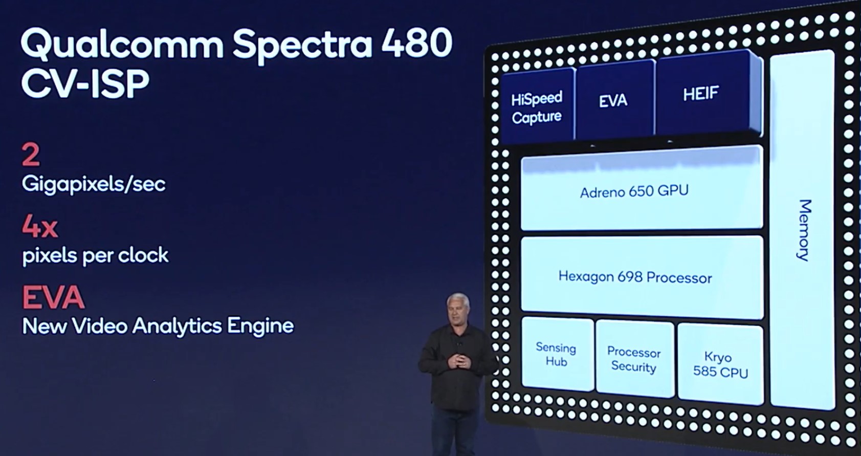
New Spectra CV-480 ISP: 2 Gigapixels/s Enabling Massive Sensors
Aside from its 5G abilities, it’s very much evident that camera is very much at the very centre of the Snapdragon 865’s new features. The whole camera subsystem has seen some massive upgrades in the IP, and amongst the biggest improvements in capability lies in the new Spectra 480 computer-vision ISP.
The new IP has seen a major architectural change in that it’s now able to process 4 pixels per clock instead of just only 1 PPC as in the previous generation. This has now massively upgraded the pixel processing throughput to 2 Gigapixels/second, allowing the SoC a wide variety of use-cases that in the past simply weren’t possible due to lack of raw power.
Starting off with video capture, the new SoC is able to now record in 4K HDR while simultaneously capturing up to 64MP still shots at the same time. But 4K video isn’t the limit anymore – and you even can say that in terms of framerate as now 4K120 recording is supported, but the Snapdragon 865 now supports 8K30 video recording.
Video recording quality continues to support all the features we’ve seen in the previous generation, meaning 10-bit and various HDR standards such as HLG, HDR10, HDR10+, but now the new SoC expands this even further with the introduction of the ability to do live recording in the Dolby Vision HDR standard. Qualcomm explains that the Snapdragon 865 not only is the first smartphone SoC to be able to do this, but it’s the first camera platform of any kind in the world, as usual Dolby Vision content right now is enabled post-capture in the editing room, rather being something that’s being natively recorded by a camera.
The new improved capabilities of the ISP and video encoder also erase some current recording limitations, for example, slow-motion video recording at 960fps is sustained indefinitely instead of being limited to a couple of seconds of real-time footage.
Although normally I wouldn’t have brought this up, MediaTek’s recent release of the Dimensity 1000 did recently popularise the discussion topic: No, the Snapdragon 865 doesn’t support the AV1 codec for video decoding. It looks like we’ll have to wait for the next generation for that.
In terms of still capture photography, the new ISP performance will now allow for support for sensors of up to 200MP, which actually don’t yet exist as Samsung’s recent 108MP behemoth is currently the largest of its class right now.
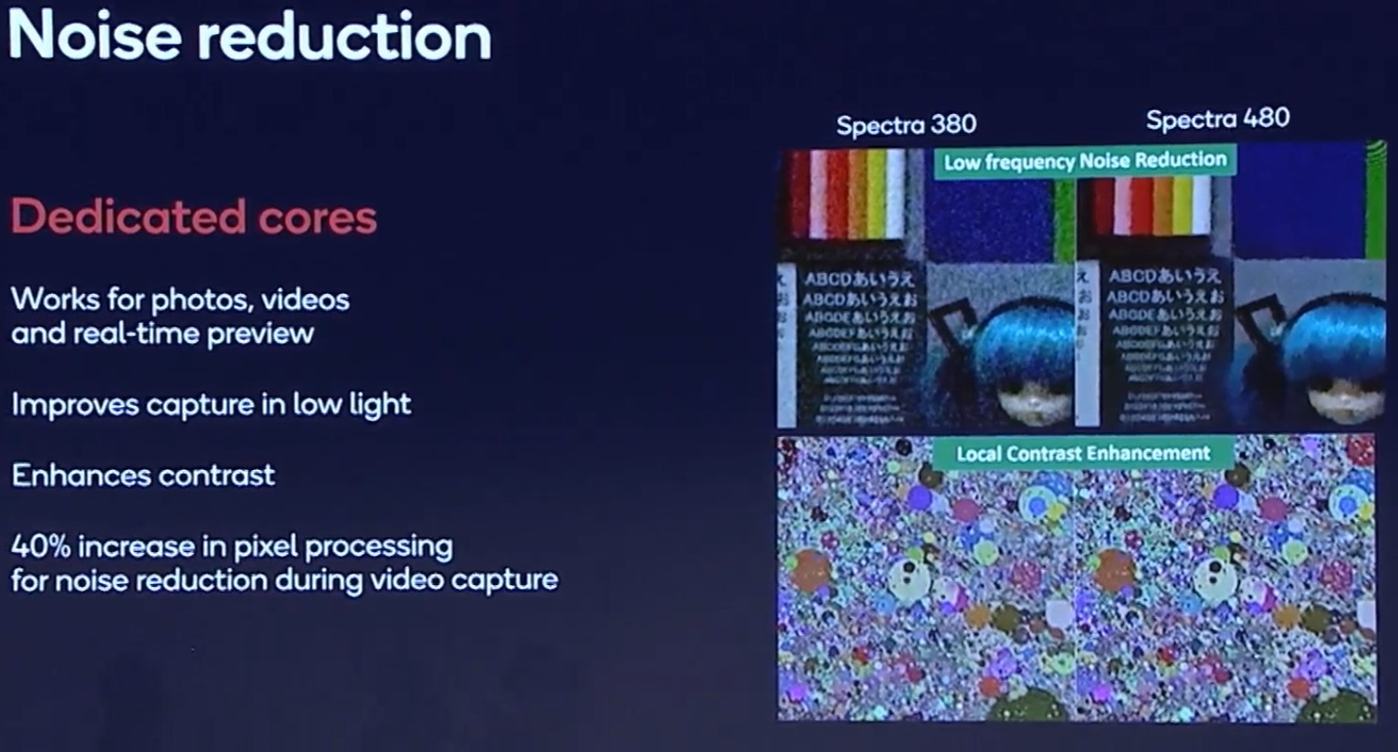
The new ISP now has various new functionalities in order to improve noise reduction and contrast enhancements. Particularly the new noise reduction features is said to be quite difficult to achieve.
Although Qualcomm advertises the 200MP figure predominantly, it’s to be noted that actual capture with zero shutter lag (ZSL) is limited to 64MP – so there is a rather larger compromise in capturing at resolutions beyond 64MP.
High Refresh Rate Displays Normalised: Support For 144Hz
Already some vendors are leading the pack in 2019, but we’re expecting 2020 to see wide-range adoption of high refresh-rate displays. Even more importantly, we’ll be seeing implementations at high resolutions higher than 90 and 120Hz, supporting up to 144Hz displays. Qualcomm explains that the barrier that’s been lifted here is the SoC’s Display Processing Unit (DPU) that has had its throughput significantly increased.
I asked the company about the impact on battery life and which component of a phone accounts for the highest power increases. Surprisingly, it’s not any one component, with most of them seeing pretty much just an evenly distributed linear increase in power requirements, with the actual display panel itself (excluding the DDIC), seeing actually the least increases in power draw.


91 Comments
View All Comments
Andrei Frumusanu - Wednesday, December 4, 2019 - link
No transistor disclosure from QC. For die sizes, we'll likely have to wait a few months.Raqia - Wednesday, December 4, 2019 - link
Quick and dirty pixel counting on this pic of a penny (19.05 mm diameter, ~285 mm^2) next to the 865 gives ~200mm^2 for the package:https://cdn.vox-cdn.com/uploads/chorus_asset/file/...
Seems like most of the budget went to the DSP, some to the GPU, and some to the larger caches. Assuming no density changes for N7P, this is about 2.76 times the die area of the 855. According to:
https://www.reddit.com/r/Damnthatsinteresting/comm...
The 855 weighs in at about 6B transistors. Quick and dirty estimate: ~16.55B transistors?
Andrei Frumusanu - Wednesday, December 4, 2019 - link
I'd gather your off in your estimate by about 8-9B transistors.Raqia - Wednesday, December 4, 2019 - link
You're probably right given this shot of the 8cx:https://scdn.slashgear.com/wp-content/uploads/2018...
which weighs in at around 10B transistors at 122mm^2 and has a larger package size. :)
tijag - Wednesday, December 4, 2019 - link
A13 manufactured on this node is 8.5B transistors, doubt strongly the 865 will be much more than that.tijag - Wednesday, December 4, 2019 - link
I see how you got to roughly 200mm^2 for the package but i'm guessing something is off on the scale or the chip is much much smaller than the BGA package its on.skavi - Wednesday, December 4, 2019 - link
I'm going to guess ~85mm^2 with ~7 billion transistors based on the image.Raqia - Wednesday, December 4, 2019 - link
You are probably right. Considering that this bump is from 6 billion - x24 modem transistors, it should be a pretty healthy gain over the 855 in GPU and DSP. Next year's TSMC 5nm process with almost double the transistor density over its 7nm processes should bring far steeper gains even with an integrated x55 modem. I'm fully expecting +75-100% performance gains in GPU and DSP with gobs more cache; their next high end part might warrant a 9xx designation.generalako - Thursday, December 5, 2019 - link
That's assuming to go over to a new architecture as well.I'm more interested about CPU(s). A78, and if ARM will actually get off their asses and give us a successor for the A55, as they seriously need to up their game here, compared to Apple -- both in terms of power efficiency and performance. I'm sure the A78 will continue the 25% IPC improvement trend, which is still very nice, but it's in an A55 successor ARM needs to do something. It's ridiculous how Apple can make a new power-efficient core every single generation, whereas ARM, whose only task is to do this, and who supplies their designs to a huge industry for far more units than iPhones, spend 3 years between them.
Raqia - Thursday, December 5, 2019 - link
There will be more straightforward gains for caches and units besides the CPU with a denser process as those workloads are more embarrassingly parallel even on the same slice/core/module architecture, and the bump from 7nm to 5nm in transistors per mobile SoC will be equal to today's mid-tier desktop GPUs.It's unclear what went into this year's vastly improved Thunder cores in the A13, but at least some of it has to do with Apple's simpler cache hierarchy and ever bigger caches with 8MB of L2 for the 2 large cores, 4MB for the 4 small cores, and a whopping 16MB for the system level L3 cache; the A77 by comparison has 512KB-256k of L2 for the big cores, 128kb of L2 for the little cores, and 4MB of L3 + 3MB of system L4. There's also the fact that they don't need to address server class Neoverse style designs as well with whatever cores they design. Having no need to integrate a modem simplifies Apple's foundry process requirements and lets it devote more die area to its CPU and caches.
As for Android CPUs at 5nm, I could see Android SoCs going to 12 cores on the CPU side or going with more cache per core / CPU complex. I don't expect as much of a single threaded performance change with the Hercules core as it'll get tougher and tougher to wring out more performance from the A76 base design that it will be based on; the successor Matterhorn though... They changed the CPU cluster design greatly with the A75+A55 combo introducing an L3 cache and have seemingly maintained this uncore through A76+A55 and A77+A55; we'll see soon enough if they have a new small design at ARM's techday in May, maybe they'll use the A65AEs next year.