Intel's Architecture Day 2018: The Future of Core, Intel GPUs, 10nm, and Hybrid x86
by Dr. Ian Cutress on December 12, 2018 9:00 AM EST- Posted in
- CPUs
- Memory
- Intel
- GPUs
- DRAM
- Architecture
- Microarchitecture
- Xe
It has been hard to miss the fact that Intel has been vacuuming up a lot of industry talent, which brings with them a lot of experience. Renduchintala, Koduri, Keller, Hook, and Carvill, are just to name a few. This new crew has decided to break Intel out of its shell for the first time in a while, holding the first in a new tradition of Intel Architecture Days. Through the five hours of presentations, Intel lifted the lid on the CPU core roadmaps through 2021, the next generation of integrated graphics, the future of Intel’s graphics business, new chips built on 3D packaging technologies, and even parts of the microarchitecture for the 2019 consumer processors. In other words, it's many of the things we've been missing out on for years. And now that Intel is once again holding these kinds of disclosures, there’s a lot to dig in to.
Contents List
Intel covered a good amount of ground at the Architecture Day, which we’ve split into the following categories:
- The CPU Core and Atom Roadmaps, on 10nm
- The Sunny Cove Microarchitecture
- The Next Generation Gen11 Graphics
- Intel Demonstrates Sunny Cove and Gen11 Graphics
- Beyond Gen11 Graphics: Announcing the Xe Graphics Brand
- 3D Packaging with FOVEROS
- Intel’s first Fovoros and first Hybrid x86 CPU: Core plus Atom in 7 W on 10nm
- Ice Lake 10nm Xeon
- Intel Made Something Really Funny: Q&A with Raja, Jim, and Murthy
The CPU Core Roadmaps
It is common for companies like Intel to ask members of the press what they enjoy about announcements from Intel, Intel’s competitors, or other companies in the industry. One of answers I will never tire of saying is ‘roadmaps’. The roadmap is a simple document but it enables a company to explain part of its future plans in a very easy to understand way. It shows to the press, to customers, and to partners, that the company has a vision beyond the next product and that it expects to deliver at a rough cadence, hopefully with some markers on expected performance additions or improvements. Roadmaps are rarely taken as set in stone either, with most people understanding that they have an element of fuzziness depending on external factors.
To that end, I’ve been requesting Intel to show roadmaps for years. They used to be common place, but ever since Skylake, it has kind of dried up. In recent months Intel has shown rough datacentre roadmaps, with Cascade Lake, Cooper Lake, and Ice Lake and the next few generations. But for the Core family it has been somewhat more difficult. Depending on which analyst you talk to, a good number will point to some of the Skylake derivatives as being holding points while the issues with 10nm have been sorted out. But nonetheless, all we tend to hear about is the faint whisper of a codename potentially, which doesn’t mean much.
So imagine my delight when we get not one roadmap from Intel on CPUs, but two. Intel gave us both the Core architecture roadmap and the Atom architecture roadmap for the next few generations.
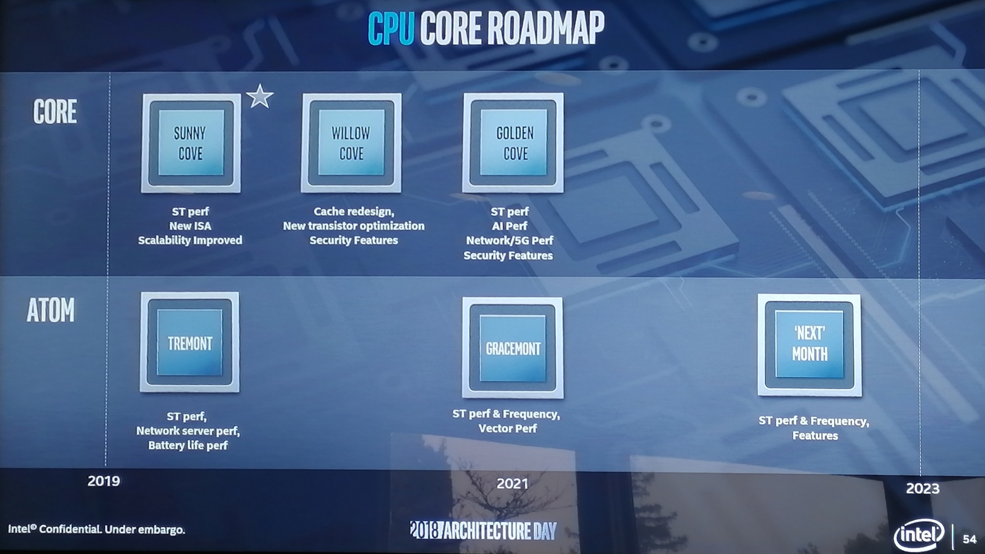
For the high performance Core architecture, Intel lists three new codenames over the next three years. To be very clear here, these are the codenames for the individual core microarchitecture, not the chip, which is an important departure from how Intel has previously done things.
Sunny Cove, built on 10nm, will come to market in 2019 and offer increased single-threaded performance, new instructions, and ‘improved scalability’. Intel went into more detail about the Sunny Cove microarchitecture, which is in the next part of this article. To avoid doubt, Sunny Cove will have AVX-512. We believe that these cores, when paired with Gen11 graphics, will be called Ice Lake.
Willow Cove looks like it will be a 2020 core design, most likely also on 10nm. Intel lists the highlights here as a cache redesign (which might mean L1/L2 adjustments), new transistor optimizations (manufacturing based), and additional security features, likely referring to further enhancements from new classes of side-channel attacks.
Golden Cove rounds out the trio, and is firmly in that 2021 segment in the graph. Process node here is a question mark, but we’re likely to see it on 10nm and or 7nm. Golden Cove is where Intel adds another slice of the serious pie onto its plate, with an increase in single threaded performance, a focus on AI performance, and potential networking and AI additions to the core design. Security features also look like they get a boost.
| Intel Core Microarchitecture Roadmap | |||
| Core Name | Year | Process Node | Improvements |
| Skylake | 2015 | 14 nm | Single Threaded Performance Lower Power Other Optimizations |
| Kaby Lake | 2016 | 14 nm+ | Frequency |
| Coffee Lake | 2017 | 14 nm++ | Frequency |
| Coffee Refresh | 2018 | 14 nm++ | Frequency |
| Sunny Cove | 2019 | 10 nm | Single Threaded Performance New Instructions Improved Scalability |
| Willow Cove | 2020 ? | 10 nm ? | Cache Redesign New Transistor Optimization Security Features |
| Golden Cove | 2021 ? | 7 / 10 nm ? | Single Threaded Performance AI Performance Networking / 5G Performance Security Features |
The lower-powered Atom microarchitecture roadmap is on a slower cadence than the Core microarchitecture, which is not surprising given its history. Seeing as how Atom has to fit into a range of devices, we’re expecting there to be a wide range in capabilities, especially from the SoC side.
The upcoming microarchitecture for 2019 is called Tremont, which focuses on single threaded performance increases, battery life increases, and network server performance. Based on some of the designs later in this article, we think that this will be a 10nm design.
Following Tremont will be Gracemont, which Intel lists as a 2021 product. As Atom is designed to continually push both the performance at the high-end of its capabilities and the efficiency at the low-end, Intel lists that Gracemont will have additional single threaded performance and a focus on increased frequency. This will be combined with additional vector performance, which likely means that Atom will get some wider vector units or support new vector instructions.
Beyond this will be a future ‘mont’ core (and not month as listed in the image). Here Intel is spitballing what this new 2023 core might have, for which the general listing of performance, frequency and features is there.
| Intel Atom Microarchitecture Roadmap | |||
| Year | Process | Improvements | |
| Goldmont | 2016 | 14 nm | Higher Performance Cryptography Features |
| Goldmont Plus | 2017 | 14 nm | Branch Prediction More Execution Larger Load/Store Buffers More Cache |
| - | 2018 | - | - |
| Tremont | 2019 | 10 nm ? | Single Threaded Performance Network Server Performance Battery Life |
| - | 2020 | - | - |
| Gracemont | 2021 | 10 nm ? | Single Threaded Performance Frequency Vector Performance |
| - | 2022 | - | - |
| 'Next Mont' | 2023 | ? | Single Threaded Performance Frequency 'Features' |
As stated above, these are just the microarchitecture names. The actual chips these cores are in will likely have different names, which means a Lake name for the Core microarchitecture. At the event, Intel stated that Ice Lake would have Sunny Cove cores in it, for example.
Another aspect to Intel’s presentations was that future microarchitectures are likely to be uncoupled from any process technologies. In order to build some resiliency into the company’s product line moving forward, both Raja Koduri and Dr. Murthy Renduchintala explained that future microarchitectures will not be process dependent, and the latest products will come to market on the best process technologies available at the time. As a result we’re likely to see some of the Core designs straddle different manufacturing technologies.
Intel also went into a bit of detail on microarchitecture of Sunny Cove.


148 Comments
View All Comments
johannesburgel - Wednesday, December 12, 2018 - link
"We have a new method inside the company to decouple IP from the process technology. You must remember that customers buy the product, not a transistor family. It’s the same transformation AMD had to go through to change the design methodology when they were struggling."...doesn't that basically mean they're going fabless, or are at least going to develop a design for multiple processes so they can also use other fabs as well? Not that I'm disagreeing with that! If I was Intel I would have started doing so years ago, when everybody else was starting to do it.
anonomouse - Wednesday, December 12, 2018 - link
I think this just means fewer hand placed/routed custom logic blocks, and more synthesis/APR. If you look at most other dies these days, you see a sea of gates. When you look at intel dies, in the cpu cores you see very tight, regular logic blocks. Every mention of "abstraction" in the Q&A screamed synthesis/APR. This may make it possible for them to port to other foundries if they wanted to, but I doubt they would.An interesting question is whether this has any implications to power/timing/area optimization vs. the current approach, as a lot of their ability to push very high clocks might come from how much more custom logic design goes into their implementation.
kapg - Wednesday, December 12, 2018 - link
I guess in the image Intel 'CPU Core Roadmap' for Atom the name 'Next' Month is a typo from IntelAlexvrb - Wednesday, December 12, 2018 - link
"quad-channel memory controller (4x16-bit)"Well, we know the GPU won't be competitive with upcoming ARM designs, then. Otherwise, very neat mobile class chip design.
Arbie - Wednesday, December 12, 2018 - link
"Golden Cove ... is firmly in that 2021 segment ... we’re likely to see it on 10nm and or 7nm."Likely? If it isn't one of those two it will be big news indeed.
HStewart - Thursday, December 13, 2018 - link
10nm is already stated for Sunny Cove in 2019, so it likely 7nm - but keep in mind the process (nm) is decouple for process - so it could be 10nm or 7nmajc9988 - Wednesday, December 12, 2018 - link
Ian, the active interposer isn't new, and I am wanting o know more exactly what has been moved to the active interposer. AMD's whitepapers on the topic, using routers, etc., on an active interposer, was published in 2014 and a follow up on 2015. In late 2017, AMD published a white paper dealing with the costs of doing so, where producing an active interposer on smaller than 40nm resulted in costs being the same as producing a monolithic die. AdoredTV did two videos on this topic months ago, as a matter of fact. So, unless they are sticking some of the features that AMD put on the I/O die onto the active interposer, this is doing what AMD plans to do but chose not to on the basis of cost. Check out these papers and videos:http://www.eecg.toronto.edu/~enright/micro14-inter... http://www.eecg.toronto.edu/~enright/Kannan_MICRO4... https://youtu.be/G3kGSbWFig4 https://seal.ece.ucsb.edu/sites/seal.ece.ucsb.edu/... https://www.youtube.com/watch?v=d3RVwLa3EmM&t=...
Intel seems to now be using ideas from everywhere else in the industry, while also using 22nm fabs that would have been slated for decommission if not for the 10nm fiasco that is their process, which they had to push certain chipsets to due to the 14nm shortage, meaning they need to keep the fab time full to justify them keeping the lights on and a 22nm active interposer fits the bill. The article practically writes itself.
iwod - Thursday, December 13, 2018 - link
No news on opening up TB3? Which they promised to do in 2018.The Hybrid, I wish it had two HP Core. but 7W is actually the same TDP for MacBook Air Retina.
The_Assimilator - Thursday, December 13, 2018 - link
Thunderbolt is dead in mainstream PCs at this point, because there's no use-case in which it outperforms USB by enough to justify its cost (both of implementation and in the peripherals that people actually want to use). It's become another almost-Mac-exclusive like Firewire, and will share the same fate.gamerk2 - Thursday, December 13, 2018 - link
Yep, this pretty much the same thing that happened to Firewire. Thunderbolt never had a reason to exist; USB3 handles pretty much every TB3 use-case.