Intel's 10nm Cannon Lake and Core i3-8121U Deep Dive Review
by Ian Cutress on January 25, 2019 10:30 AM EST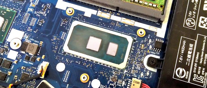
Anyone interested in leading edge semiconductors knows that Intel is late with its newest manufacturing process. The '10nm' node was first announced in 2014, to be released in 2016. While officially 'shipping for revenue' by 31 December 2017, the only way we knew to get hold of an Intel 10nm x86 CPU was if you happened to be a Chinese school and work with a specific distributor to buy a specific laptop.We pulled in a few favors from within the industry and managed to source the laptop for review.
Intel's Sole 10nm Processor
The single processor from Intel built on 10nm falls under the Core 8th generation family, and is called the Core i3-8121U. The cores are built with Intel's Cannon Lake microarchitecture, a variant of the Skylake architecture built on 14nm, and it is manufactured as a dual core with integrated graphics. The part nominally has a standard 'GT2' graphics configuration, but is actually shipped without the graphics enabled - some analysts believe that this is because it doesn't work (see more on the next page). Norminally this is a 2+2 design (two cores, GT2 graphics), however it might also be referred to as a 2+0 design.
| Intel 10nm Cannon Lake CPUs | ||||||
| Cores | Base Freq |
Turbo Freq |
Graphics | DRAM | TDP | |
| Core i3-8121U | 2 (4) | 2.2 GHz | 3.2 GHz | None (GT2 Fused Off) |
DDR4-2400 LPDDR4-2400 |
15W |
The two cores run at a 2.2 GHz base frequency at 15W thermal design power, and offers a 3.2 GHz turbo frequency. Memory support includes LPDDR4, one of very few Intel processors to do so, but also this processor has AVX-512 capabilities, allowing it to process vector math much like Intel's Enterprise class hardware but now in a low end chip. We'll dive deep into all these points in this review.
What Do We Have
The sole laptop which has an Intel Core i3-8121U inside is a specific model of the Chinese Lenovo Ideapad E330-15ICN.

The advert from the listing
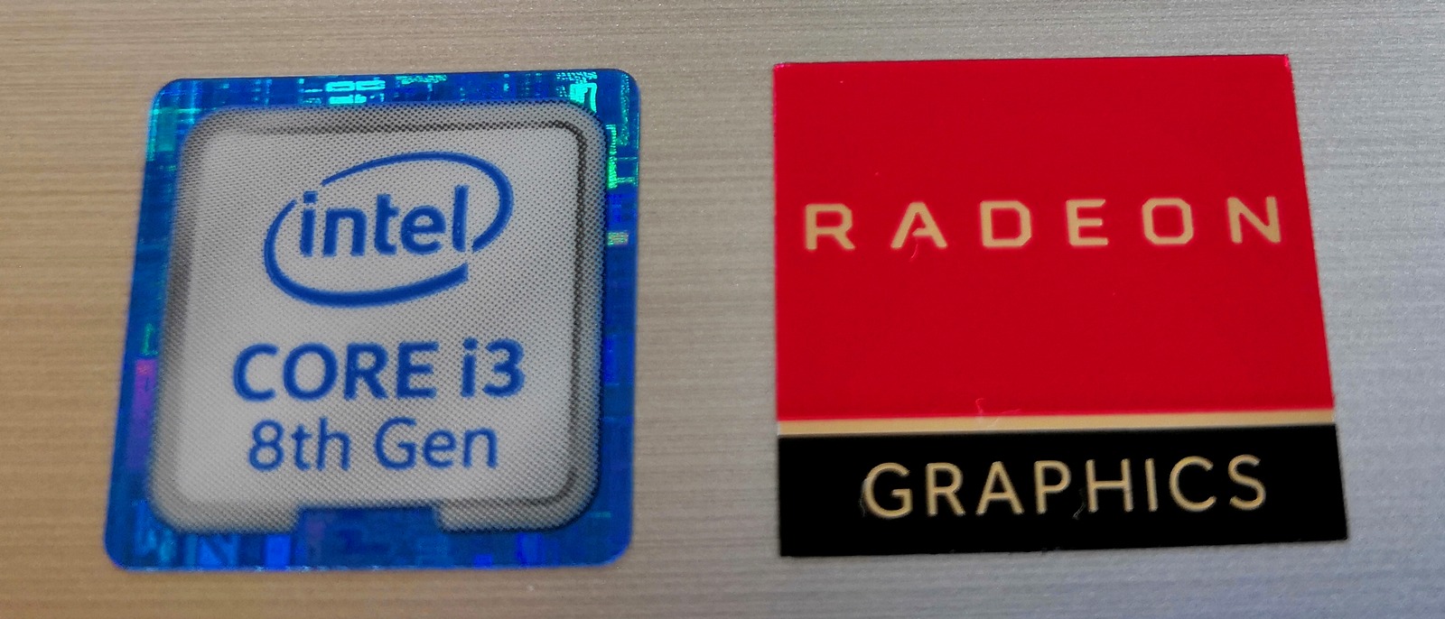
This is an educational focused device, with educational focused specifications - a 15.6-inch screen running at a 1366x768 resolution with a TN panel (with limited viewing angles), a small 33.4 Wh battery, 8GB of DRAM, a 256GB SSD, and a 1TB mechanical hard-drive. Because the chip has no integrated graphics, Lenovo had to add a physical GPU, which will be the same one as found in the upcoming NUC: AMD's Radeon RX540. This adds another 50W thermal design power to the whole unit, which complicates the cooling system considerably compared to a standard 15W CPU on its own. Along the educational theme, it also comes with an ethernet port, a HDMI port, two USB ports, a 3.5mm jack, a Type-C USB connector, a 720p webcam, a microSD card slot, an 802.11ac Wi-Fi module, and an optional DVD slot (which loses the second SATA HDD).
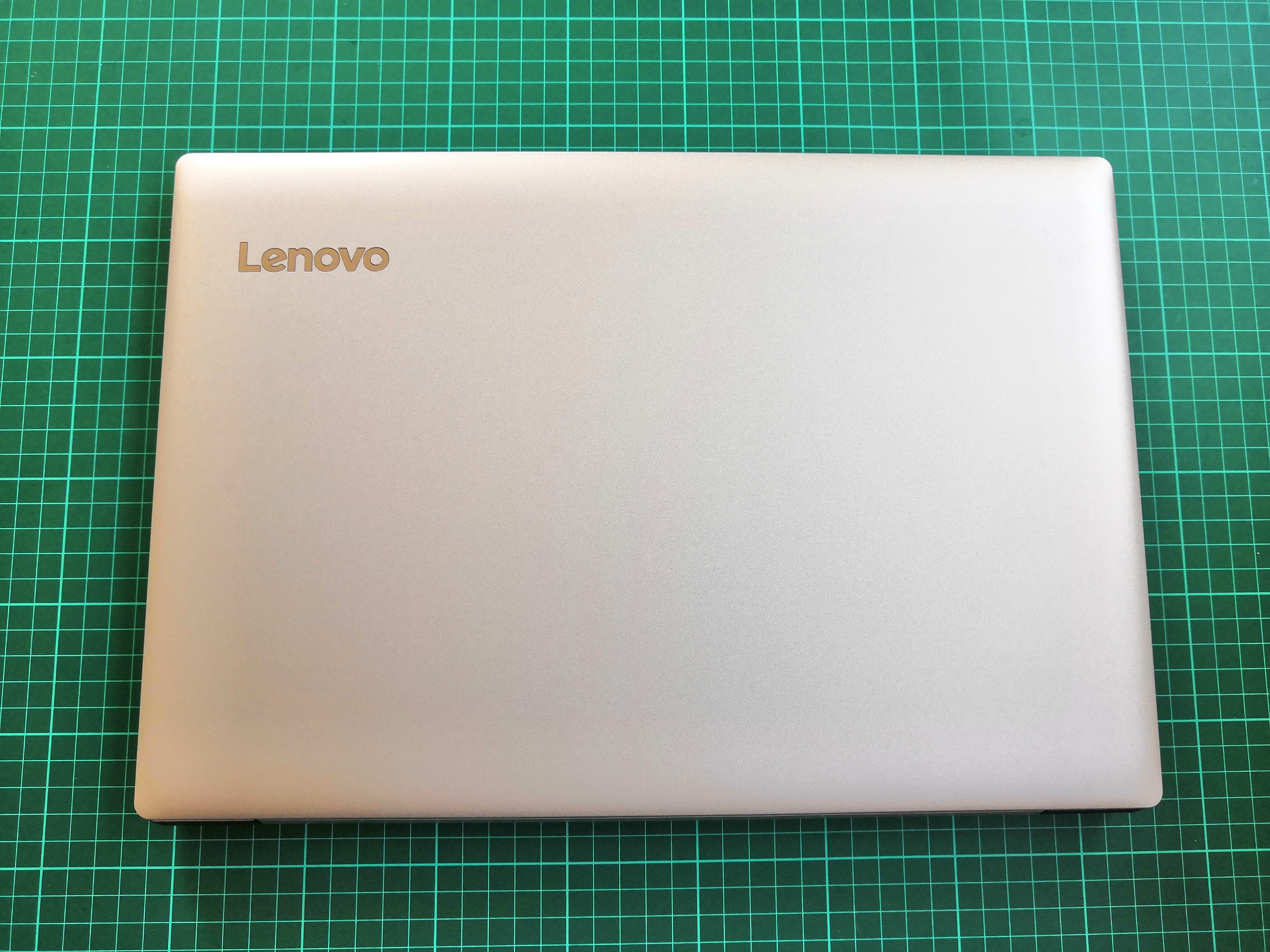
The design is very unassuming. The grey finish means that it won't stand out at Starbucks, aside from the bulk of a heavy 15.6-inch device. As is perhaps to be expected, it feels very utilitarian. No-one is buying this for looks or for style.
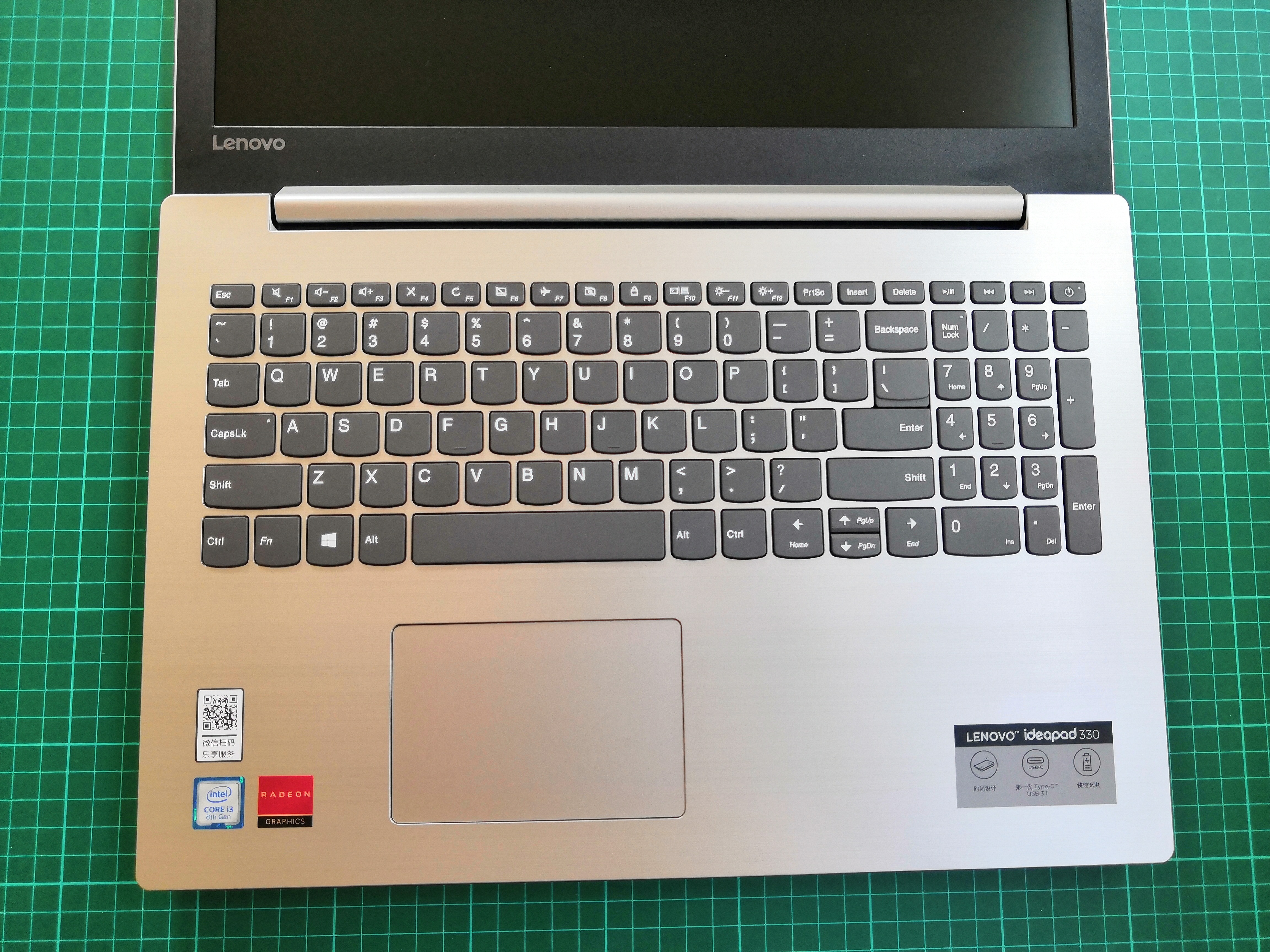
The keyboard fits in with the cost-down implementation here, although having used it for a few events to take notes, it is very usable. Despite being a Chinese device, we ended up with a US keyboard, but with half-height arrow buttons. The keypad is also present, with some media keys at the top. Unfortunately the power key is on the top right, above the minus sign, making it very easy to hit for prolific users of a keypad.

On the top is the webcam. This unit has massive bezels for the display, which contributes a lot to the bulk of the system. The webcam is usable for meetings at least, and the microphones do work but are cheap as we expect.

Welcome to the heart - Intel Core i3 plus AMD Radeon graphics. Sadly not an impressive combination like Kaby G.
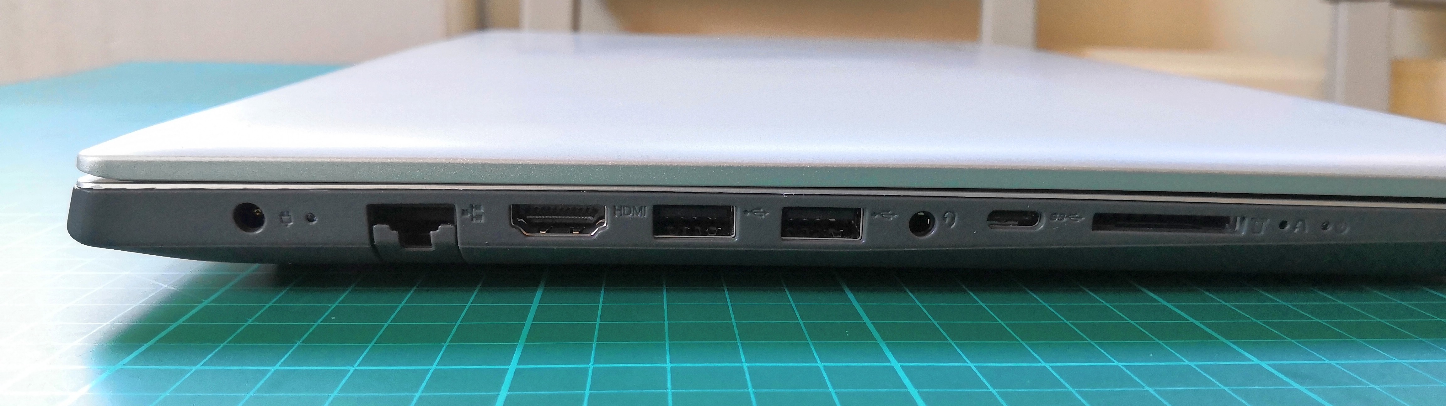
On the sides are all of the ports. They are all located on the left side, and include the power connector, the gigabit Ethernet port, a HDMI port, two USB ports, a 3.5mm jack, a Type-C USB port, and an SD card slot. On the other side of the unit is the removable bay.
On the rear, we get intakes at the front, and an intake in the middle of the bottom of the chassis. There are small rubber feet to help lift the laptop when on a table, but these do not really help on a lap. Given the amount of heat that needs to be dissipated in this system, this isn't great - the exhaust is found in the hinge between the main body and the display. The fan inside has to cope with all of this, as we'll see in a bit.

Going inside the system, and removing the removable bay, looks a bit like this.
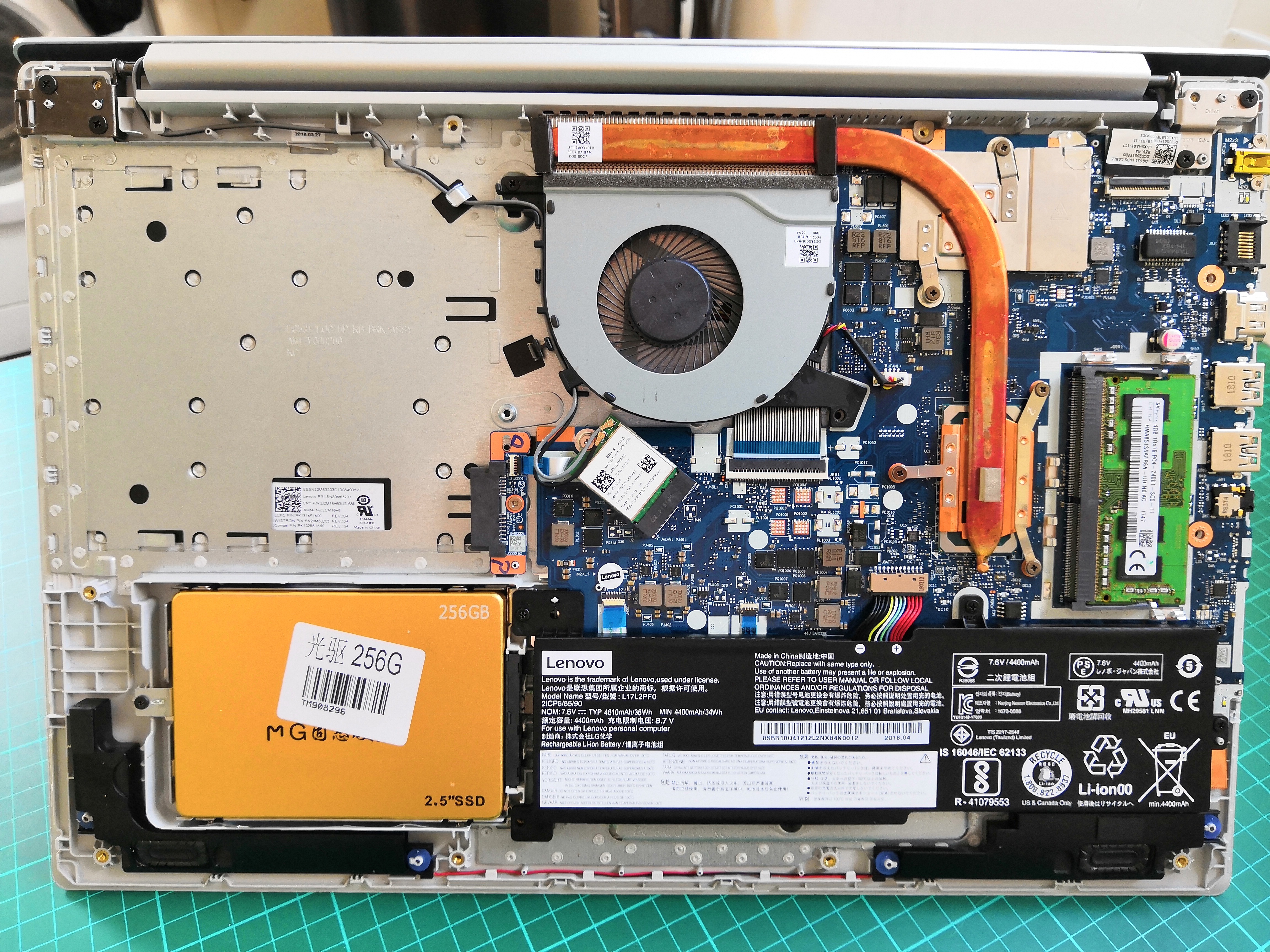
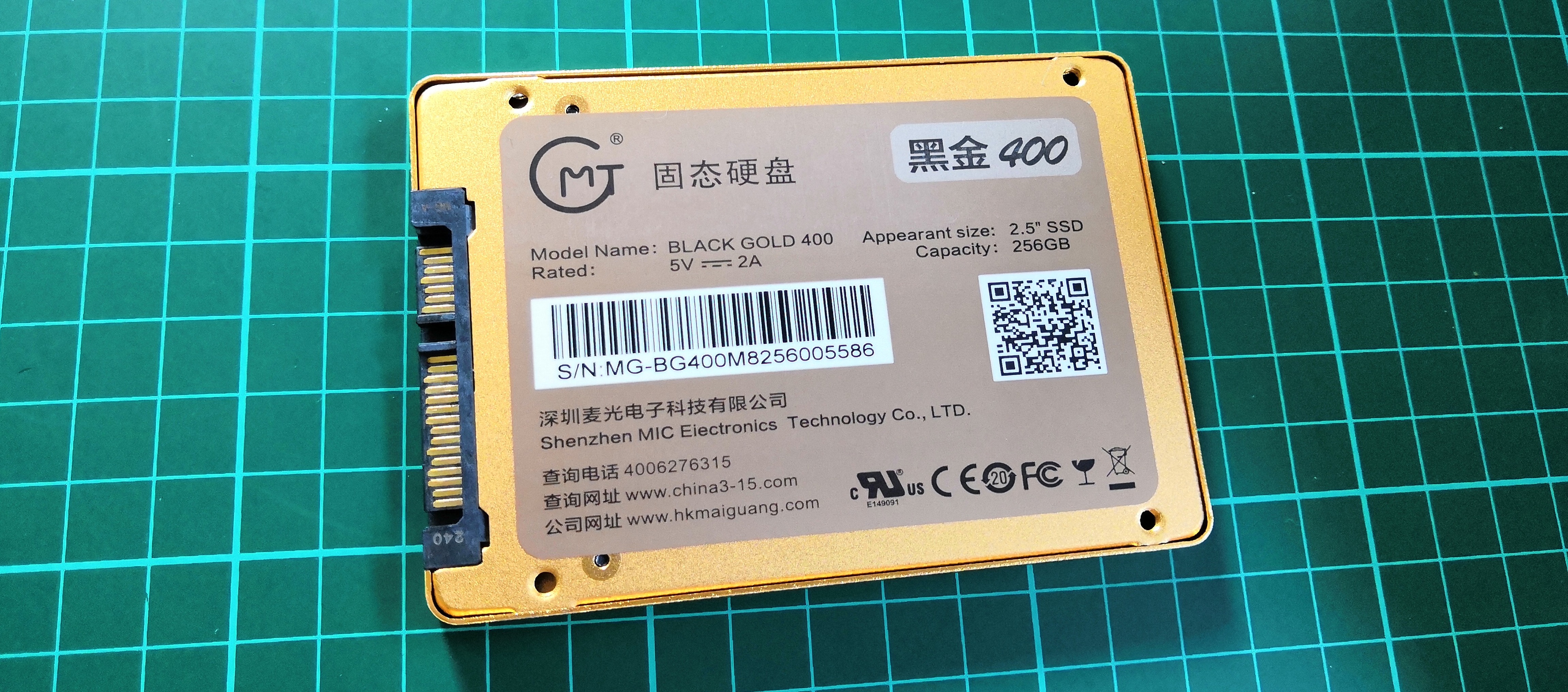
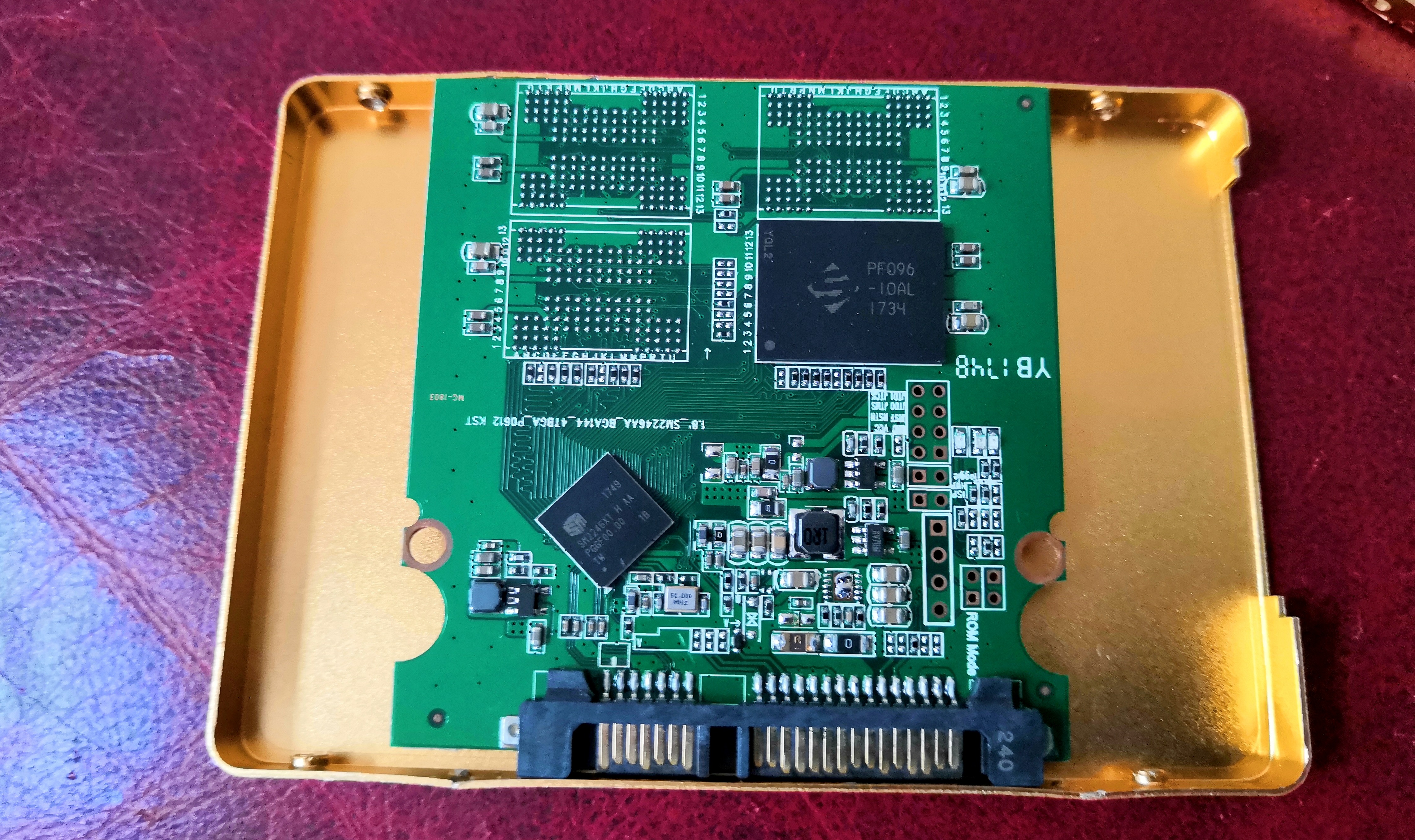
On the left is the 256GB SSD, branded as an 'MT Black Gold 400' drive in a 2.5-inch chassis. This unit is very gold. It is a budget drive, featuring the DRAM-less Silicon Motion SM2246XT controller combined with Spektek NAND flash (rebadged cheap Micron NAND). This unit is clearly part of a series of SSDs, given the number of empty pads. But I guess even having an SSD is still an interesting upgrade over a purely mechanical drive.
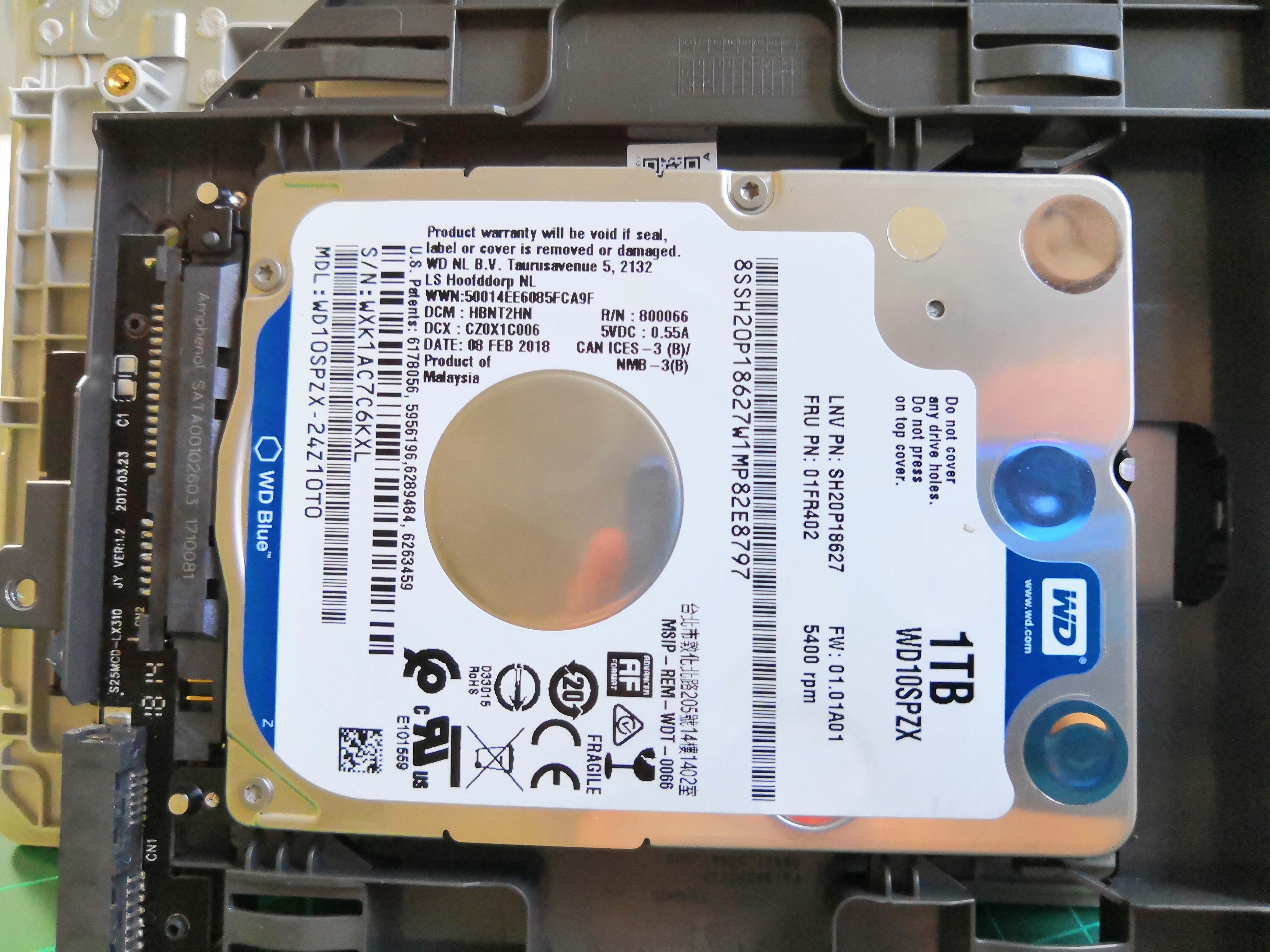
The other drive in the system, not pictured in the main image, is spinning rust - a 1TB WD Blue. This is actually pretty commendable to have this drive in a system like this, although the 5400RPM platter speed means that it will be slow for almost everything. It makes me wonder if drives like this should be using the SSD as a caching technology instead.
The WiFi module has a Lenovo part number but underneath is a Realtek RTL8821CE 802.11ac module, supporting 433 Mbps speed (1T1R) and Bluetooth. This is an M.2 module, which means it could be upgraded at a later date fairly easily. It is a dual band module, which as an educational system should be more than suitable for the classroom that has an access point close by.

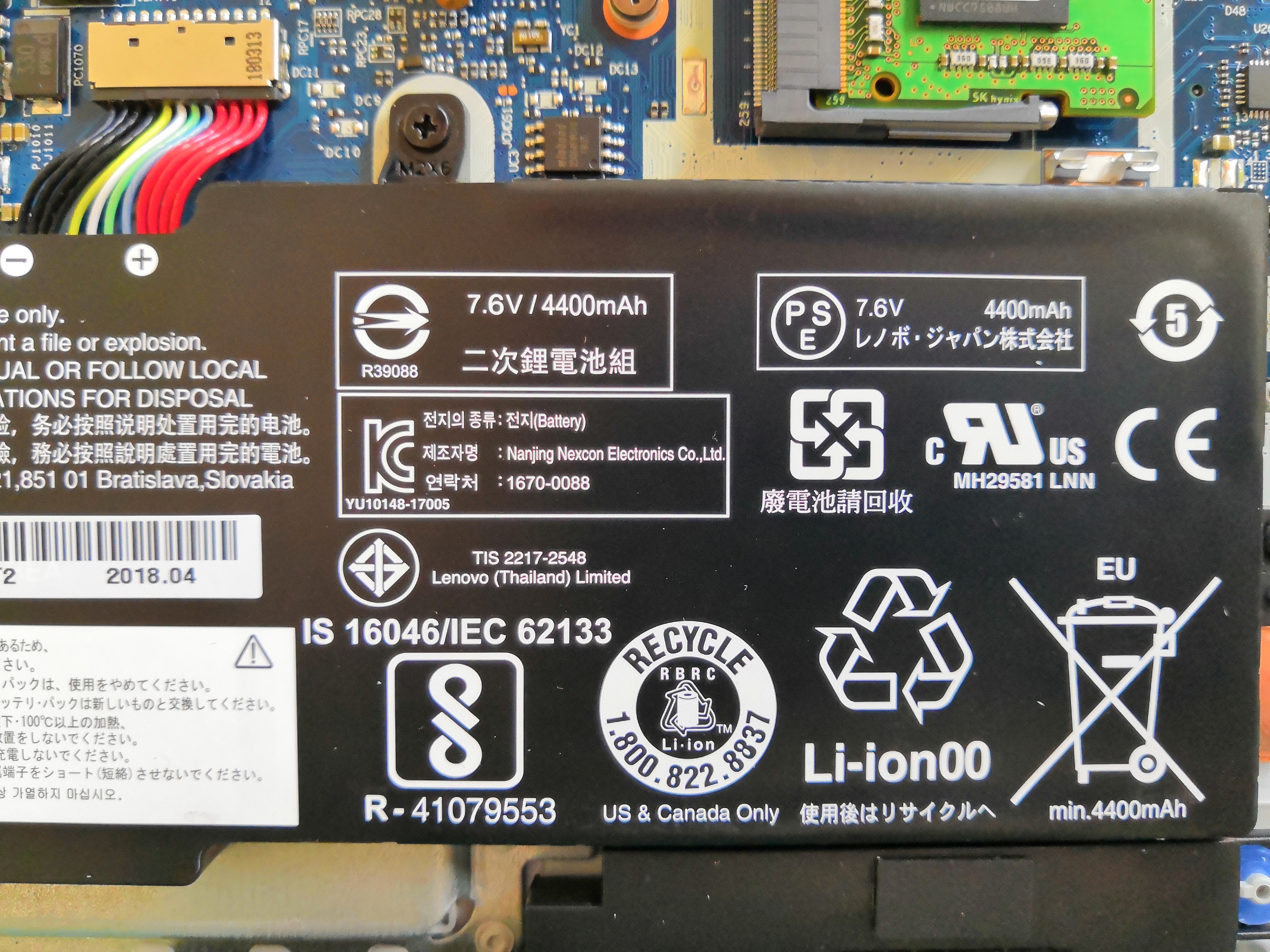
The battery, as mentioned above, is a tiny battery. The 33.4Wh lithium-ion unit is a 2-cell device, which equates to 4400 mAh at 7.6 V, and is made for Lenovo in Thailand by the Nanjing Nexcon Electronics Co.
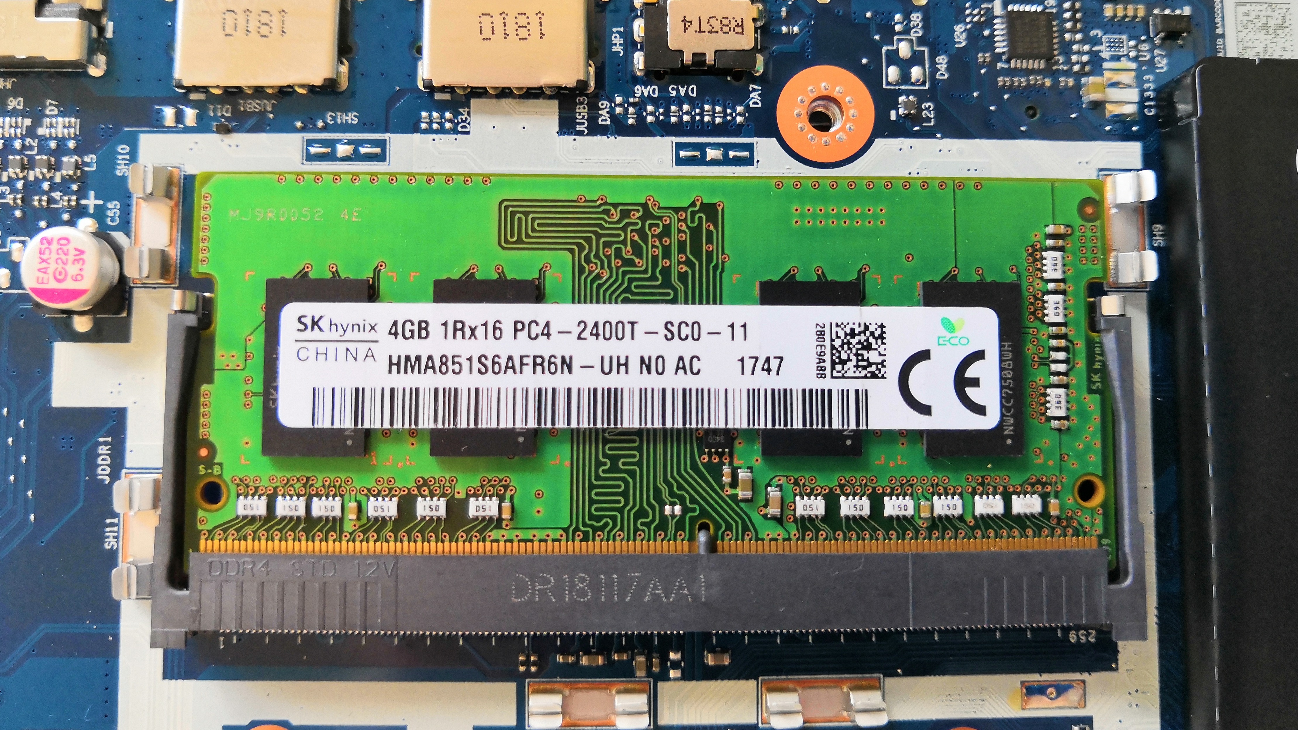
For system memory, the unit has 4GB soldered onto the rear of the PCB, and offers a single SO-DIMM slot for an additional module. The base configuration for this device has 4GB of memory in single channel mode, however up to 16GB more can be added. The configurations we were offered showed another 4GB module, bringing the total up to 8GB. Again, having 8GB of DRAM in an educational device probably sits about right, and kudos for them being in dual channel as well.
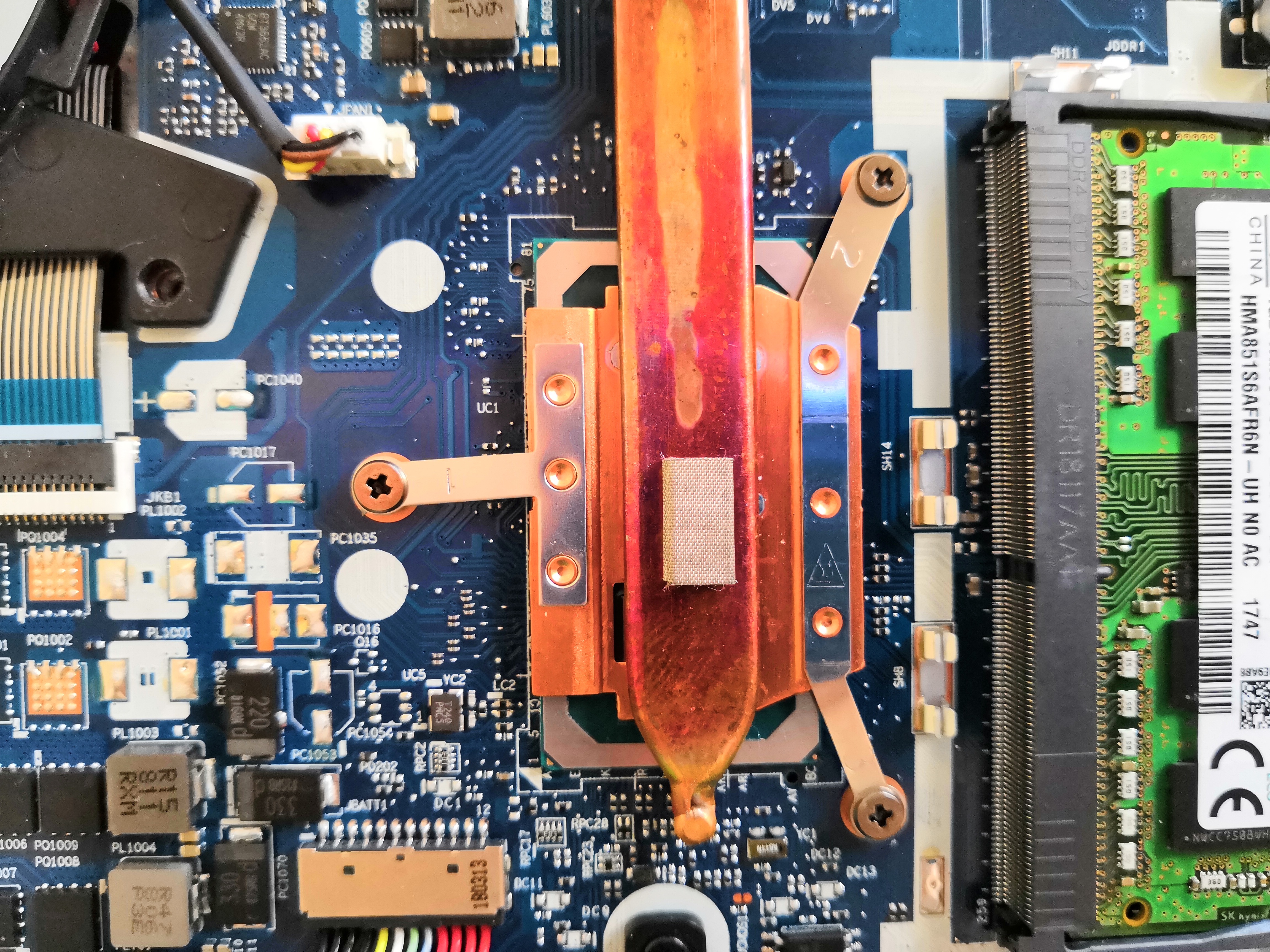
The meat of the laptop, the CPU and GPU, are found near the center and have blower cooling. Despite the 15W TDP of the CPU and the 50W TDP of the GPU, there is a single flat heatpipe going from the CPU to the GPU and to the heatsink connected to the thin blower fan. This feels like a cheap fan paired with aluminum fins. This feels woefully inadequate for such the system, and the power consumption combined with the small battery leads to interesting figures for battery life. In thermals, the system does get warm to the touch around the cooler area, which is thankfully a little way away from the keyboard and not really felt when active.
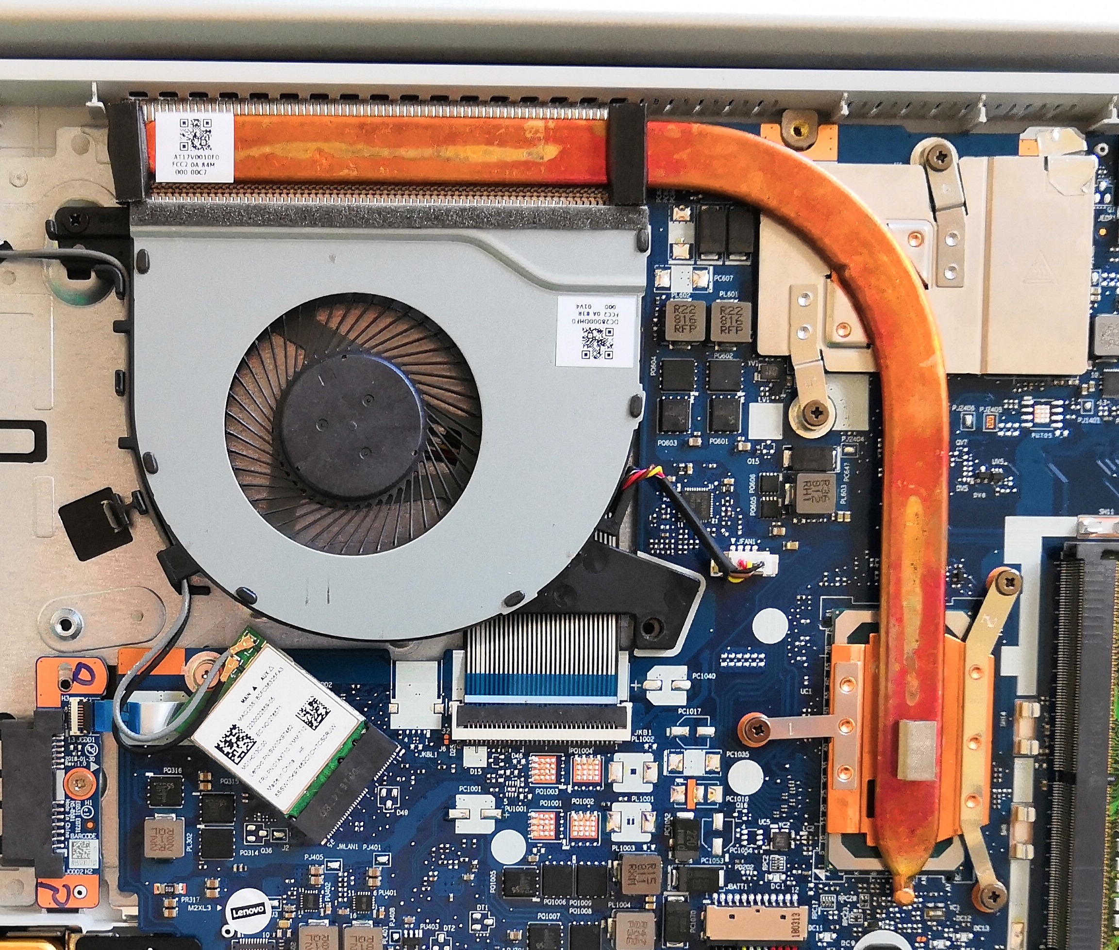
The GPU area has a sizable copper heatsink fixed in two spots to the PCB.
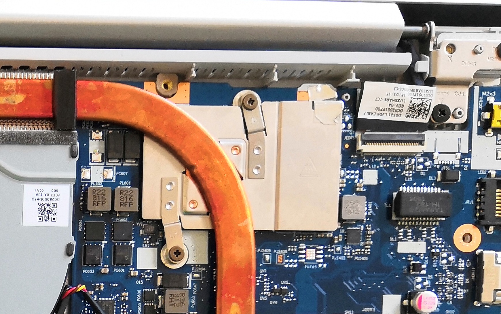
The CPU area is instead attached at three points, and there is an additional pad to stop the chassis from rubbing against the heatpipe. This means that the chip height combined with the PCB and the heatsink is enough to start to worry how the chassis brushes up against the internals? Interesting.
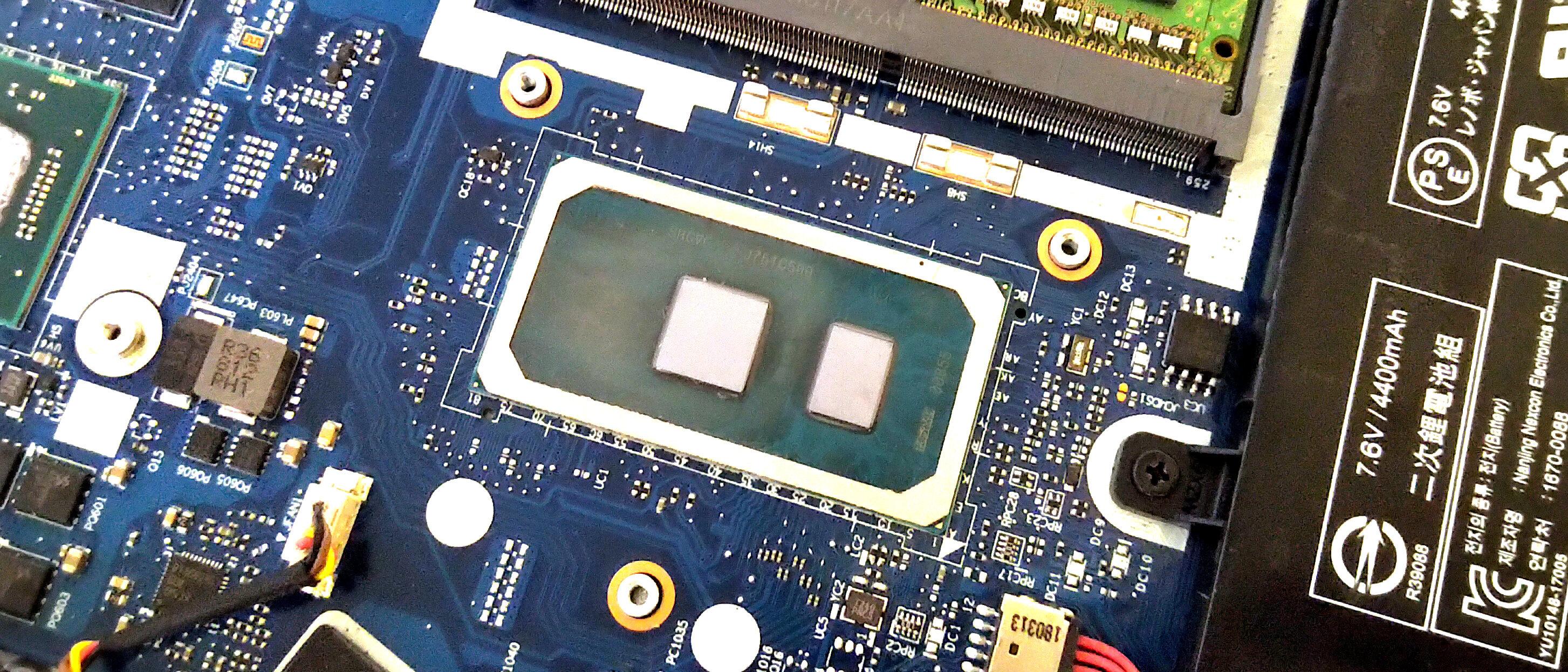
Underneath the heatsink is this chip. What we have here is the 2+2 die from Intel (with graphics disabled, so 2+0 as shipped), along with the chipset. Back when Intel showed off a full wafer of these chips, we calculated a rough die size of 8.2mm by 8.6mm, or 70.5mm2 per die. In actual fact, we were essentially accurate in our estimation. This means there can be up to 850 dies per 300mm wafer. How many of those actually work at the level Intel wanted? That would be a fun question to have answered.
The base model of this device retailed for around $450 from our source in China - that's the 4GB model with a 500GB HDD. With the extra memory (up to 8GB) and storage (256GB SSD + 1TB HDD) the cost to us was around $650, plus postage. It took about six weeks to get the device, after calling in a few favors from friends in the region. For everyone else, a NUC was recently released onto shelves in December.
This Review
Within this article we want to do several things. Firstly, discuss and describe the history behind Intel's 10nm plans, the claims and the marketing, as well as what we currently know about what is in this 10nm Cannon Lake processor. Then we will go into what Cannon Lake brings to the table in its microarchitecture based on what we can find out, using tools, microbenchmarks, and also calling in some investigative experts. Following this is some benchmarks - we want to look into both generational improvements and chip production performance increases, coming at the performance angle but also a nod towards power and memory performance. Finally we'll end with a discussion about the future of this version of Intel's 10nm.
It should be noted that Intel did not offer or provide the device for this article - we purchased this device ourselves. When asked about diving deeper into the design of the chip about a month ago, Intel never really responded to my request. I currently have a more recent request to discuss the topic, and I'm waiting on a response.


129 Comments
View All Comments
yeeeeman - Saturday, January 26, 2019 - link
As someone said it earlier in this thread, I think we miss opportunities when moving to a new process every two years. The mishap that Intel had just showed us how much better a process can become if you give the time to your engineers. 14nm started late, with some low clocked parts. We had some Broadwell chips that ran at 3.3 base. Then, Skylake came and the 6700k brought 4ghz at quite high power. Then, the 7700k came and another tweak to the process improved clocks, so we now got 4.7 GHz boost. After this, things moved up in core counts (which should've happen a long time ago, but with competition...) and we got 8700k and now 9900k with turbo to 5ghz. Until now, only 32nm with Sandy Bridge came close to 5ghz mark. Now, with a lot of time to tweak, they have become so confident in the 14nm process that they released a 5ghz stock cpu. Financials say the true story. Even if we cry about 10nm, truth is that things can move forward without a new process. It is cheaper actually to prolong the life of a certain process and if they can add enough improvements from generation to generation, they can afford to launch new process once every 4-5 years.Dodozoid - Saturday, January 26, 2019 - link
Indeed, we probably have to get used to a lot of +++ processes. During the architecture day, the new Intel people (old AMD people) mentioned they are decoupling the architecture from the process. That means they can make progress other than pushing clocks on the same core over and over, but IPC as well...KOneJ - Sunday, January 27, 2019 - link
Unfortunately, SB-derivatives seem to be needing a significant overhaul. "tocks" of late haven't exactly brought meaningful IPC gains. Hopefully deeper and wider *Cove designs are a step in the right direction. I just don't like that Intel seems to be taking an approach not dissimilar to the Pentium 4 the last time AMD reared its head. Only this time, a major departure in micro-architecture and steady process advantage isn't in the wings. Even with the *Coves, I think AMD may be able to build enough steam to solidly overtake them. There's no reason that Zen 4 and on couldn't go deeper and wider too, especially looking at power consumption on the front and back ends of the Zen core versus the uncore mesh. I think Zen derivatives currently will try the wider first. It actually might make the high core-count parts significantly more power efficient. Also could easily scale better than post-SB did if Agner Fog's analysis is anything to go by. Multiple CPU die masks and uncore topologies incoming? Wouldn't surprise me.dgingeri - Saturday, January 26, 2019 - link
Well, yeah, they can be improved upon over time, but that doesn't cut the production costs like a process reduction does. improving the process can increase yields and increase performance, but only by a limited percent. A process reduction increases the number of chips from a wafer by a much higher amount, even if there are more defects.Well, that was the way it worked up until the 14nm process.
With 10nm at Intel, they had far too many defects, and the process failed to give the returns they wanted for quite a while. That had as much to do with the quality of the wafers before production as it did the production process itself. They had to push the wafer producers to higher levels of purity in order to fix that. I'm fairly sure TSMC would have had the same issues with their 7nm, but Intel had already pushed the wafer production to higher levels of purity because of their problems, so TSMC was able to take a couple extra steps ahead because of that.
These days, we're going to see each step smaller take longer and longer to get right, because of these same hurdles. As things get smaller, impurities will have a higher and higher impact on production. We may not get as far as some are hoping, simply because we can't get silicon as pure as necessary.
name99 - Saturday, January 26, 2019 - link
"Another takeaway is that after not saying much about 10nm for a while, Intel was opening up. However, the company very quickly became quiet again."The history page is great. But I have to wonder if the ultimate conclusion is that the best thing, for both Intel and the world, is that they STICK to the STFU strategy? And that journalist stick to enforcing it.
One thing that's incredibly clear from all this is that Intel are utterly lousy at forecasting the future. Maybe it's deliberate lies, maybe it's just extreme optimism, maybe it's some sort of institutional pathology that prevents bad news flowing upward?
Regardless, an Intel prediction for beyond maybe two years seems to be utterly worthless. Which raises the question -- why bother asking for them, and why bother printing them?
Look at that collection of technologies from the 2010 slide that are supposed to be delivered over the next nine years. We got Computational Lithography, and that's about it. CErtainly no III-V or Germanium or Nanowires. Interconnects (Foveros and EMIB?) well, yeah, in about as real a form as 10nm. 3D refers to what? Die stacking? or 3D structures? Either way nothing beyond the already extant FinFETs. Dense Memory? Well yeah, there's Optane, but that's not what they had in mind at the time, and Optane DIMMs are still crazy specialized. Optical Interconnect? Well occasional mutterings about on-die photonics, but nothing serious yet.
Now on the one hand you could say that prediction is hard. How much better would IBM, or TSMC, or Samsung, have done? On the other hand (and this is the point) those companies DON'T DO THIS! They don't make fools of themselves by engaging in wild claims about what they will be delivering in five years. Even when they do discuss the future, it's in careful measured tones, not this sort of "ha ha, we have <crazy tech> already working and all our idiot competitors are four years behind" asinine behavior.
I suspect we'd all be better off if every tech outlet made a commitment that they won't publish or discuss any Intel claims regarding more than two years from now. If you're willing to do that, you might as well just call yourself "Home of Free Intel's advertising". Because it's clear that's ALL these claims are. They are not useful indications of the future. They're merely mini-Intel ads intended to make their competition look bad, and with ZERO grounding in reality beyond that goal.
KOneJ - Sunday, January 27, 2019 - link
While you're correct that the media is ignorantly doing just that for the most part, at least this article provides context in what Intel is trying to do in obfuscating the numbers versus TSMC and Samsung who haven't stumbled the same way. Some of the Foveros "magic" is certainly not being knocked-down enough when people don't understand what it's intended to do. 2.5D, 3D, MCMs, and TSVs all overlap but cover different issues. I blame the uneducated reader more than anything. Good material is out there, and critical analysis between the lines is under-present. "Silicon photonics" was a big catch-phrase in calls a few years ago, but quiet now. Hype, engineering, and execution are all muddied by PR crap. Ian is however due credit for at least showing meaningful numbers. It's more in the readers hands now. Your last remarks really aren't fair to this article, even if they bear a certain degree of merit in general. Sometimes lies are needed to help others understand the truth though...HStewart - Saturday, January 26, 2019 - link
I believe that this Cannon is get AVX 512 out to developers. What would be interesting if possible is for Intel to release Covey Lake on both 14nm and new 10nm. One thing I would expect that Covey Lake will significant speed increase compare to current 14nm chips even if on 14nm and the 10nm will be also increase but combine Covey Lake and new 10nm+. should be quite amazing.One test that I am not sure is benchmark that runs in both AVX2 and AVX 512 and see the difference. There must be reason why Intel is doing the change.
KOneJ - Sunday, January 27, 2019 - link
Cheap Cannon Lake is not designed to get AVX512 into dev hands. That's the dumbest thing ever. And "Covey Lake"? Please read the article before commenting. There are a few good blog posts and whitepapers out there analyzing and detailing SIMD across AVX varieties. For most things, AVX512 isn't as big a deal as earlier SIMDs were. It has some specialized uses as it is novel, but vectoring code and optimizing compilers to maturity is slow and difficult. There are fewer quality code slingers and devs out there than you would expect. Comp sci has become littered with an unfortunate abundance of cheap low-quality talent.HStewart - Sunday, January 27, 2019 - link
Ok for the misunderstood people about AVX 512 - which appear to be 2x fast AVX2https://www.prowesscorp.com/what-is-intel-avx-512-...
yes it going to take a while people user AVX 512 - but just think about it twice the bits - I was like you not believe 512 but instead 64 bit would make in days of early 64 bit - thinking primary that is will make program largers and not necessary. As developer for 3 decades one thing I have send that 64 bit has done is make developer lazy - more memory less to worry about in algorithms for going to large arrays.
As for Sunny Cove, it logical with more units in the chip - it is going to make a difference - of course Cannon Lake does not have Sunny Cove - so it does not count. Big difference will be seen when Covey Lake cpus come out what the difference it be like with Cannon Lake - and even Kaby Lake and assoicated commetitors chips
HStewart - Sunday, January 27, 2019 - link
One thing on Covey Lake and upcoming 7nm from Intel, it is no doubt that it designers made a mistake with Cannon Lake's 10nm - Intel realizes that and has created new fabs and also new design architexture - there is no real reason for Intel to release a Cannon Lake - but it good to see that next generation is just more that Node change - it includes the Covey Lake architexture change.