Intel Officially Reveals Post-8th Generation Core Architecture Code Name: Ice Lake, Built on 10nm+
by Ian Cutress on August 15, 2017 9:20 AM EST- Posted in
- CPUs
- Intel
- Core
- Coffee Lake
- Ice Lake
- Cannon Lake
In an unusual move for Intel, the chip giant has ever so slightly taken the wraps off of one of their future generation Core architectures. Basic information on the Ice Lake architecture has been published over on Intel's codename decoder, officially confirming for the first time the existence of the architecture and that it will be made on Intel's 10nm+ process.
This is an unexpected development as the company has yet to formally detail (let alone launch) the first 10nm Core architecture – Cannon Lake – and it's rare these days for Intel to talk more than a generation ahead in CPU architectures. Equally as interesting is the fact that Intel is calling Ice Lake the successor to their upcoming 8th generation Coffee Lake processors, which codename bingo aside, throws some confusion on where the 14nm Coffee Lake and 10nm Cannon Lake will eventually stand.
As a refresher, the last few generations of Core have been Sandy Bridge, Ivy Bridge, Broadwell, Haswell, Skylake, with Kaby Lake being the latest and was recently released at the top of the year. Kaby Lake is Intel’s third Core product produced using a 14nm lithography process, specifically the second-generation ’14 PLUS’ (or 14+) version of Intel's 14nm process.
Meanwhile when it comes to future products, back at CES Intel briefly showed a device based on post-Kaby Lake designs, called Cannon Lake and based on their 10nm process. Since then Intel has also confirmed that the 8th Generation of processors for desktops, called Coffee Lake, will be announced on August 21st (and we recently received promotional material to that effect). Ice Lake then, seems poised to follow both Coffee Lake and Cannon Lake, succeeding both architectures with a single architecture based on 10nm+.
Working purely on lithographic nomenclature, Intel has three processes on 14nm: 14, 14+, and 14++. As shown to everyone at Intel’s Technology Manufacturing Day a couple of months ago, these will be followed by a trio of 10nm processes: 10nm, 10nm+ (10+), and 10++,
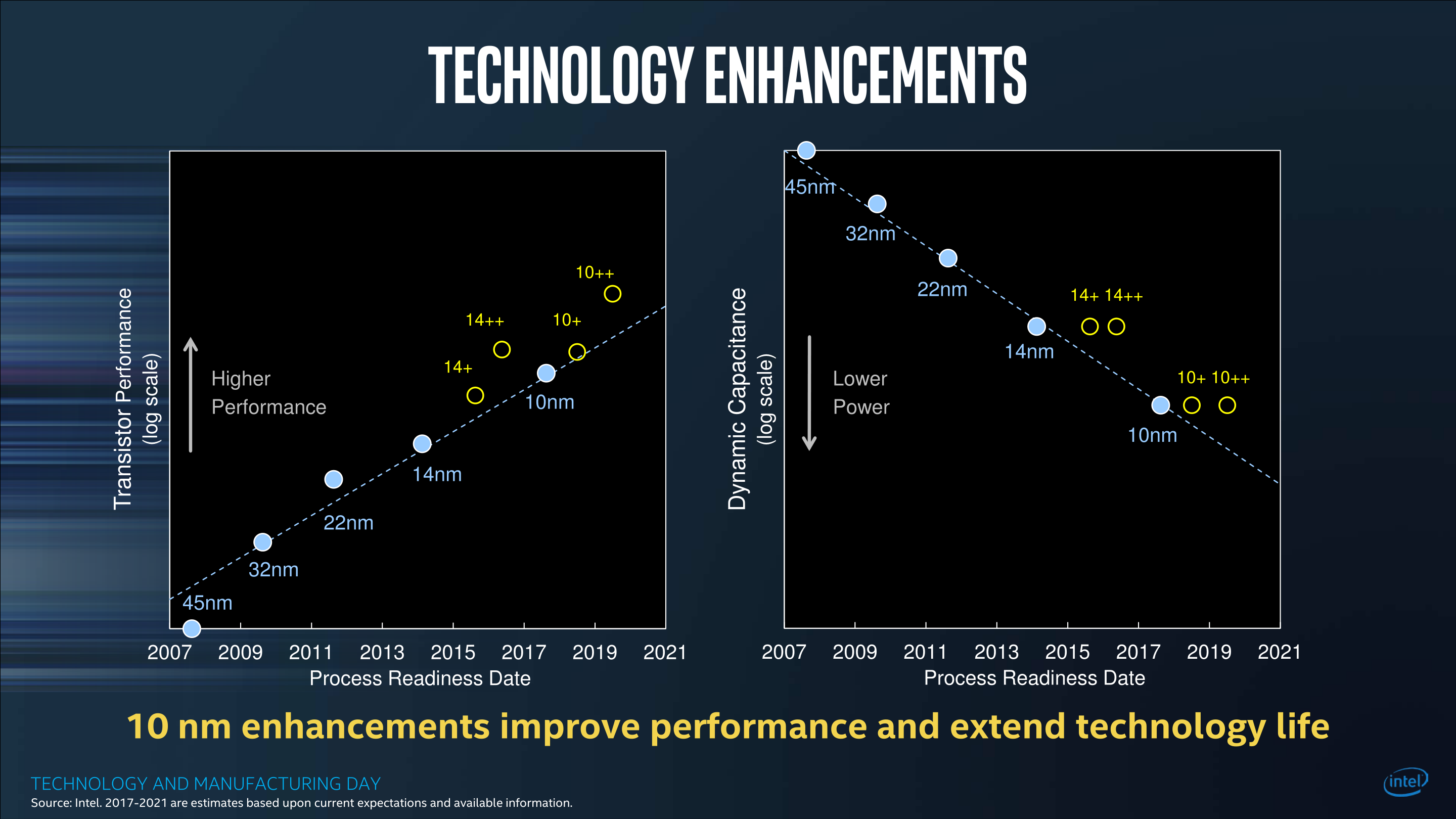
On the desktop, Core processors will go from 14 to 14+ to 14++, such that we move from Skylake to Kaby Lake to Coffee Lake. On the Laptop side, this goes from 14 to 14+ to 14++/10, such that we move from Skylake to Kaby Lake to Coffee Lake like the desktops, but also that at some time during the Coffee Lake generation, Cannon Lake will also be launched for laptops. The next node for both after this is 10+, which will be helmed by the Ice Lake architecture.
| Intel's Core Architecture Cadence | |||||
| Microarchitecture | Core Generation | Process Node | Release Year | ||
| Sandy Bridge | 2nd | 32nm | 2011 | ||
| Ivy Bridge | 3rd | 22nm | 2012 | ||
| Haswell | 4th | 22nm | 2013 | ||
| Broadwell | 5th | 14nm | 2014 | ||
| Skylake | 6th | 14nm | 2015 | ||
| Kaby Lake | 7th | 14nm+ | 2016 | ||
| Coffee Lake | 8th | 14nm++ | 2017 | ||
| Cannon Lake | 8th? | 10nm | 2018? | ||
| Ice Lake | 9th? | 10nm+ | 2018? | ||
The way that the desktop and laptop markets will be diverging then converging is confusing a lot of people. Why is the laptop market splitting between 14++ and 10, and why is the desktop market not going to 10nm but straight to 10+? What lies beyond is a miasma of guess work, leaked slides, and guessing Intel’s strategy, but I believe the answer lies in Intel’s manufacturing technologies and the ability to move to newer lithographic nodes.
(We should interject here that the naming of a lithographic node has slowly lost its relevance between the features of the process and the actual transistor density and performance, such that TSMC’s improved 16FF+ is called 12FFN, but relies on similar transistor sizes with enhanced attributes. But 12 is a smaller number than 14, which is the marketing angle kicking in. By all accounts, Intel has typically been considered the more accurate foundry when it comes to numerical lithographic naming of the process, which others consider is to their detriment.)
Intel originally predicted that they would move to 10nm almost a year ago, at the end of 2016 and 2 years after the launch of their 14nm process. But the challenge in managing the technology required to advance to their version of 10nm has been fraught with difficulty. In all cases it can depend on external equipment, fine tuning a process, or getting acceptable yields – while one manufacturer might be satisfied with an 80% yield, another might consider that a failure. Being able to obtain high yields (ramp up) will also be a function of die size, and so the newest nodes are typically launched with smaller mobile parts in mind first, as the yields for smaller parts are better than larger parts at the same defect rate.
Simply put, the first generation of 10nm requires small processors to ensure high yields. Intel seems to be putting the smaller die sizes (i.e. anything under 15W for a laptop) into the 10nm Cannon Lake bucket, while the larger 35W+ chips will be on 14++ Coffee Lake, a tried and tested sub-node for larger CPUs. While the desktop sits on 14++ for a bit longer, it gives time for Intel to further develop their 10nm fabrication abilities, leading to their 10+ process for larger chips by working their other large chip segments (FPGA, MIC) first.
From a manufacturing standpoint, Intel has been using multiple patterning techniques in its 14nm processes, and the industry is looking to when the transition to EUV will take place. Anton has some great writeups of the state of EUV and how different companies are transitioning to smaller nodes - they are well worth a read.
- EUV Lithography Makes Good Progress, Still Not Ready for Prime Time
- Samsung and TSMC Roadmaps: 8 and 6 nm Added, Looking at 22ULP and 12FFC
- GlobalFoundries Updates Roadmap: 7 nm in 2H 2018, EUV Sooner Than Later?
The crux of the matter is that EUV would shorten time to market and arguably make the process easier (if only more expensive), and several fab companies are waiting for Intel to jump onto it first. With EUV not ready, Intel has had to invest into deeper multi-patterning techniques, which raise costs, decrease yields, and increase wafer process times considerably.
All of which leads to a miasma of increased delays, much to the potential chagrin of investors but also customers who had banked on the power improvements that a typical new lithography node brings. Intel is still keeping spirits high, by producing numbers that would suggest that their methodology is still in tune with Moore’s Law, even if the products seem to be further strung out. Some analysts concur with Intel’s statements, while others see it as hand-waving until 10/10+ hits the market. Intel would also point out that it is developing other technologies such as Embedded Multi-Die Interconnect Bridges (EMIB) to assist in equipping chip with high-speed fabric or glue-logic.
Given its position as a post-8th gen architecture, Ice Lake is likely to hit sometime in 2018, perhaps 2019, depending on Intel’s rate of progress with larger chips and the 10+ process. Intel’s other market segments, such as FPGAs (Altera), Xeon Phi (MIC) and custom foundry partners, are also in the mix to get into some 10nm action.
(Note that Intel’s next generation of Xeon Scalable Processors is called Cascade Lake, a 2018 refresh of the Skylake generation launched this year.)


Source: Intel


106 Comments
View All Comments
BurntMyBacon - Wednesday, August 16, 2017 - link
Stevo's post actually suggests that even if they did push hardware requirements in games, hardware performance has not progressed sufficiently to meet that demand (at least in CPUs). I suppose GPU's are still moving at a reasonable pace (though not as fast as they once were) and developers could make better use of the resources available. However, the fact that you can still draw a valid comparison between a third generation core processor and an 8th generation core processor at all should tell you how little progress CPUs have made on the performance front. Now, if you want to talk about power efficiency and cost (manufacturing, not necessarily retail), that's a different story.philehidiot - Wednesday, August 16, 2017 - link
Yeah fair enough. I didn't read it like that but on a re-read I can see how you'd come to that conclusion. I was referring more to GPUs and being held back, the CPU comment was a poorly thought through afterthought and you're probably right. As for GPUs, looking at the FPS you get out of the latest games with a 1080 these days it's just silly. I remember when we were using the Crysis games as a benchmark and GPUs were struggling to get playable frame rates at high settings. I'm sure that with the lack of any real competition, Intel have been simply putting as little R&D as possible in to ensure something useful comes out, whilst adding in the occasional extra "feature" like the next version of HDCP and changing the socket so as to screw over their customers. I'm not a fan of any particular brand and I certainly won't advocate for one product over another based on anything other than objective criteria.... but I really don't like the way Intel does business. I don't know if AMD are genuinely any better but to me they have a better company image. Maybe it's the whole "liking the under dog" thing.Interested to hear what you think about manufacturing costs. They're making out that it's getting harder and harder with yields getting lower and lower with each process shrink yet you seem to imply that this isn't the case and CPUs are getting cheaper to make?
BurntMyBacon - Wednesday, August 16, 2017 - link
You are correct, manufacturing has gotten harder. This was particularly apparent with the Broadwell line and may show up again with Cannon Lake. However, die sizes have also gotten smaller. Outside the ridiculously priced low volume Broadwell-E i7-6950X, prices have largely remained stagnant between generations. Combine this with the fact that Intel's margins have remained lofty and it suggests that the overall cost to manufacture has remained somewhat stable despite all the troubles. Also, keep in mind that yields improve over the life of a process. Now that Intel is sticking with the same process node 3 and 4 generations, it would seem that costs should be dropping for the same sized chunk of silicon using the same or extremely similar manufacturing methods. I acknowledge that things are rarely as simple as they seem, but complexity is usually at odds with reducing cost, so I'm probably painting a pretty conservative picture here.As far as 14+ and 14++ go, they strike me as marketing terms needed to counter the other foundries' so called smaller processes. Intel has always made improvements to their process over time, they just have more time to make additional improvements this time. Just like every other time, I expect yields will continue to improve despite (or because of) the changes.
tienchien1 - Sunday, August 20, 2017 - link
What's your job?In business, anyone will do as intel. We are not gods.
StevoLincolnite - Thursday, August 17, 2017 - link
It's a Sandy Bridge-E chip.It's actually 2nd Gen Core. :P
Here is a comparison between Sandy Bridge-E and Broadwell-E. (Sadly Anandtechs bench doesn't let me compare against Skylake-X.)
http://www.anandtech.com/bench/product/1727?vs=552
The difference is inconsequential.
Then if we compare Broadwell-E and Skylake-X... Performance still hasn't moved much.
http://www.anandtech.com/bench/product/1727?vs=190...
5-6 years... And if I spent almost $1,000 AUD on a new CPU, Board and Ram I wouldn't even get a 50% improvement.
BurntMyBacon - Thursday, August 17, 2017 - link
@StevoLincolnite: "It's a Sandy Bridge-E chip.It's actually 2nd Gen Core. :P"
I was thinking 2nd Gen, but my hands were typing 3rd Gen. In any case, it just makes it that much more impressive. Kudos to you for getting the right system at the right time.
HollyDOL - Friday, August 18, 2017 - link
I upgraded from i5-2500K to i5-6400 (non OCed, cpu died) and have to say the performance is the same. These days it's more about features you can get (access to) than raw performance... old board had 2x6Gbps + 4x3Gbps sata, new one has several PCIe M.2s, all SATA ports are 6Gbps etc. Regardless, if the old one didn't die, I'd still be using it.BurntMyBacon - Wednesday, August 16, 2017 - link
@StevoLincolnite: "With my 1866Mhz DDR3 modules, I have more bandwidth than Dual-Channel DDR4 3200Mhz."Also, at lower latency IIRC.
@StevoLincolnite: "Only thing that is a let down is that it only has Sata 6Gbit rather than 16Gbit.
And no USB 3.1, USB C. - But you can live without that, not worth the rush to upgrade."
Not sure what you'd plug into a SATA 16Gbit (SATA Express). I haven't seen any drives use it. All the M.2 SATA drives I've seen use 6Gbit controllers even if the interface should be capable of supporting faster. I'd just grab a PCIe to M.2 adapter card and throw a PCIe M.2 drive on it. You should have more than enough lanes on your platform to support this and the interface will be faster than any SATA standard.
They do have USB 3.1 adapter cards. Again, I see no reason you board wouldn't have enough PCIe lanes to support this should it become desirable in the future. No need to live without it if you want it.
@StevoLincolnite: "It's insane how long this rig has lasted me and it's still got a ton of life left in it."
Yeah, maybe more than you've considered. You could probably ride that system until something breaks without it feeling shamefully outdated (assuming periodic video card upgrades).
StevoLincolnite - Thursday, August 17, 2017 - link
I was just listing off checklist features that I don't have... And you are right, USB 3.1 cards are available. And I do have plenty of PCI-E Lanes. Back with Sandy Bridge-E, Intel didn't castrate the amount of PCI-E lanes on the hex chips.Lolimaster - Wednesday, August 16, 2017 - link
Except you can now get the Ryzen 7 1700 with 50%+ more performance while consuming 3 times less... and with upgrades all the way to 2020.