Samsung and TSMC Roadmaps: 8 and 6 nm Added, Looking at 22ULP and 12FFC
by Anton Shilov on May 5, 2017 9:30 AM EST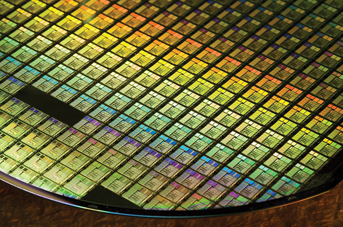
Samsung and TSMC made several important announcements about the present and future of their semiconductor manufacturing technologies in March. Samsung revealed that it had shipped over 70 thousand wafers processed using its first-generation 10 nm FinFET fabrication process (10LPE) and also announced major additions to its upcoming manufacturing technology roadmap. In particular, the company plans to introduce three processes it has not talked about thus far. TSMC said that it is about to start mass production of ICs (integrated circuits) using its first-gen 10 nm technology and also announced several new processes that will be launched in the coming years, including its first 7 nm EUV process due in 2019.
10 nm: Samsung Is Shipping
Update 5/12: Samsung informed us that its press release from October, 2016, compares characteristics of the 10LPE manufacturing technology with those of the 14LPE, not 14LPP. The text and table have been updated accordingly.
Samsung said it had started to make SoCs using its 10LPE fabrication technology last October, which is something we already knew. This manufacturing process allowed the company to make its chips 30% smaller compared to ICs made using its 14LPE process as well as reducing power consumption by 40% (at the same frequency and complexity) or increase their frequency by 27% (at the same power and complexity). So far, Samsung has processed over 70 thousand wafers using its 10LPE technology, which can give an idea about Samsung’s 10 nm production capacities (considering that the whole 10 nm production cycle is greater than the 90 days we saw with previous-gen FinFET processes). At the same time, keep in mind that Samsung does not have many 10 nm designs to manufacture right now: we know only of the company’s own Exynos 9 Octa 8895 as well as Qualcomm’s Snapdragon 835 seen in the Samsung Galaxy S8.
| Advertised PPA Improvements of New Process Technologies Data announced by companies during conference calls, press briefings and in press releases |
||||||||
| GF | Samsung | |||||||
| 7nm DUV vs 14LPP |
14LPP vs 28LPP |
10LPE vs 14LPE |
10LPE vs 14LPP |
10LPP vs 10LPE |
10LPU vs 10LPE |
|||
| Power | >60% | 60% | 40% | 30% | ~15% | ? | ||
| Performance | >30% | 40% | 27% | >10% | ~10% | ? | ||
| Area Reduction | >50% | 50% | 30% | 30% | none | ? | ||
In addition to its production milestone, Samsung also confirmed plans to start mass production of chips using its second-generation 10 nm manufacturing process called 10LPP (10 nm low-power plus) by the end of 2017 as well as its third-generation 10 nm technology called 10LPU by the end of 2018. Samsung said last year that the 10LPP is going to enable a ~10% performance increase (at the same power and at the same complexity) versus the 10LPE, but we know absolutely nothing about the 10LPU. It is logical to assume that the 10LPU will bring certain PPA-related (performance, power, area) improvements, but it is not clear how Samsung plans to achieve them and which one of the three will be the focus for improvements. As it appears, just like Intel, Samsung has ended up with three generations of 14 nm fabrication processes and is going to end up with three generations of 10 nm manufacturing technologies. It is noteworthy that Samsung itself does not use its 14LPC (low-power compact) for its leading edge SoCs, which may suggest that the 10LPU is also not aimed at this segment of the market. In fact, it is highly likely that the 10LPU will target ultra-small and ultra-low-power ICs for various emerging devices, but Samsung yet has to confirm that.
10nm: TSMC Is Steady
As for TSMC, its 10 nm process technology (CLN10FF) is now qualified for production at the company’s GigaFabs 12 and 15, where high-volume ramp is expected to start in H2 2017. Production capacity of these two fabs is hundreds of thousands wafer starts per quarter and TSMC plans to ship 400 thousand wafers processed using its 10 nm manufacturing tech this year. Considering the long production cycles for FinFET-based technologies, it is about time for TSMC to start ramping up 10 nm so to be able to supply enough chips to its main customer in time. Apple is expected to launch its new iPhone products in September or October and needs to get SoCs couple of months before the launch.
| Advertised PPA Improvements of New Process Technologies Data announced by companies during conference calls, press briefings and in press releases |
|||||||
| TSMC | |||||||
| 16FF+ vs 28HPM |
16FF+ vs 20SOC |
10FF vs 16FF+ |
7FF vs 16FF+ |
7FF vs 10FF |
|||
| Power | 70% | 60% | 40% | 60% | <40% | ||
| Performance | 65% | 40% | 20% | 30% | ? | ||
| Area Reduction | ~50% | none | >50% | 70% | >37% | ||
PPA advantages of TSMC’s CLN10FF over its CLN16FF+ (second-gen 16 nm) have been discussed already and they are significant for developers of mobile SoCs (but not that significant for makers of other ICs): a ~50% higher transistor density, a 20% performance improvement at the same power and complexity or a 40% lower power consumption at the same frequency and complexity. Unlike Samsung, TSMC does not seem to plan multiple generations of 10 nm and will go straight to 7 nm next year. 7nm is currently very popular among chip designers, indicating a future major milestone. However, in addition to the CLN7FF, the company will also offer several other manufacturing technologies for ultra-small and ultra-low-power applications.


89 Comments
View All Comments
mdriftmeyer - Friday, May 5, 2017 - link
Being 63.63 times smaller in diameter for an atom compared to the fab process is quite a large span in scale.boeush - Saturday, May 6, 2017 - link
One thing to consider, though, is that when atoms are bound into molecules via covalent bonds, the distances between their nuclei shrink below the sum of the adjacent atoms' stand-alone radii: in other words, chemically bound atoms pack together much more tightly than one might naively expect by conceptualizing each atom as a solid sphere...Jon Tseng - Friday, May 5, 2017 - link
PSA: NODES WITH THE SAME (NUMERICAL) NAME FROM DIFFERENT VENDORS ARE NOT EQUIVALENT.Just wanted to get that out of the way early! :-p
Meteor2 - Friday, May 5, 2017 - link
Indeed. The x nm labels are meaningless now; they may as well call them Bob and Joan.The only way to compare them is via the inter-node PPA change metrics. Anyone have numbers for 22->14 and 14->10 from Intel to hand?
Even then I know Intel's 14 nm is better on at least power and performance than others' 14/16 nm, as the latter are actually 20 nm with FinFET added, but I'm not aware of any meaningful way of comparing them.
lefty2 - Friday, May 5, 2017 - link
That's not totally true. The first iteration of Intel's 14nm performed worse than TSMC's 16nm. 14nm+ is much better thoughDrumsticks - Friday, May 5, 2017 - link
I'm not calling you wrong or anything, but can you source that? Intel's original 14nm might have had bad yields for a while, but I imagine it's difficult to compare outright performance without published numbers, given that Intel's 14nm went into CPUs with a frequency of 800MHz to 4.5 GHz, versus TSMC's biggest wins being Apple and GPUs, none of which went past the low 2GHzs. Obviously it's difficult to compare performance on frequency with something like that.SuperMecha - Saturday, May 6, 2017 - link
See page 4. There are probably several other factors that determine performance other than leakage and drive current.https://newsroom.intel.com/newsroom/wp-content/upl...
Meteor2 - Sunday, May 7, 2017 - link
Good link, and a good quote within:"Industry “10 nm” technologies are expected to ship sometime in 2017 and have similar density to Intel’s 14 nm technology that has been shipping since 2014."
helvete - Thursday, July 20, 2017 - link
Would you expect anything else from Intel paper? (Not telling they are far from the truth)lefty2 - Saturday, May 6, 2017 - link
The first iteration of 14nm was Broadfield and Broadfield did not clock to 4.5GHz. Also, you can't compare to a smartphone SoC, which have to keep within a very small power envelope.