Intel Confirms 8th Gen Core on 14nm, Data Center First to New Nodes
by Ian Cutress on February 9, 2017 6:52 PM EST- Posted in
- CPUs
- Intel
- Core 8th Gen
- Cannon Lake
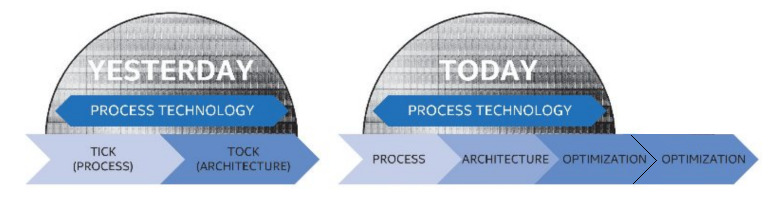
A quick news piece on information coming out of Intel’s annual Investor Day in California. As confirmed to Ashraf Eassa by Intel at the event, Intel’s 8th Generation Core microarchitecture will remain on the 14nm node. This is an interesting development with the recent launch of Intel’s 7th Generation Core products being touted as the ‘optimization’ behind the new ‘Process-Architecture-Optimization’ three-stage cadence that had replaced the old ‘tick-tock’ cadence. With Intel stringing out 14nm (or at least, an improved variant of 14nm as we’ve seen on 7th Gen) for another generation, it makes us wonder where exactly Intel can promise future performance or efficiency gains on the design unless they start implementing microarchitecture changes.
Despite this, if you were to believe supposed ‘leaked’ roadmaps (which we haven’t confirmed from a second source as of yet), the 8th Generation product ‘Cannon Lake’ is more geared towards the Y and U part of Intel’s roadmap. This would ring true with a mobile first strategy that Intel has mirrored with recent generations such that the smaller, low power chips are off the production line for a new product first, however we'd also expect 10nm to also be in the smaller chips first too (as demonstrated at CES). Where Cannon Lake will end up in the desktop or enterprise segment however remains to be seen. To put something a bit more solid into this, Ashraf also mentioned words from Dr. Venkata ‘Murthy’ Renduchintala, VP and GM of Client and IoT:
‘Murthy referred to it at the event, process tech use will be ‘fluid’ based on segment’.
If one read too much into this, we may start seeing a blend of process nodes for different segments at the same time for different areas of the market. We already do have that to some extent with the mainstream CPUs and the HEDT/Xeon families, but this phrasing seems that we might get another split between consumer products or consumer and enterprise. We may get to a point where Intel's 'Gen' naming scheme for its CPUs covers two or more process node variants.
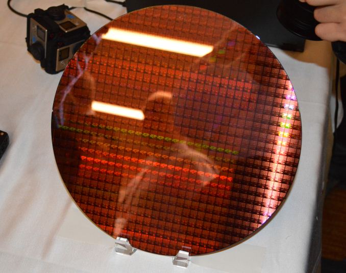
Speaking of the Enterprise segment, another bit of information has also surfaced, coming from a slide during a talk by Diane Bryant (EVP/GM of Data Center) and posted online by Ashraf. The slide contains the words ‘Data center first for next process node’

We can either talk about process node in terms of the ‘number’, either 14nm/10nm/7nm, or by variants within that process (high power, high efficiency). One might suspect that this means Intel is moving hard and fast with 10nm for Xeons and big computing projects, despite showing off 10nm silicon at CES earlier this year. That being said, it’s important to remember that the data center market is large, and includes high-density systems with many cores, such as Atom cores, and Intel did recently open up its 10nm foundry business to ARM Artisan IP projects. So while the slide does say ‘Data center first’, it might be referring to DC projects based on ARM IP in that segment rather than big 4-24+ core Xeons. At this stage of the game it is hard to tell.
On top of all this, Intel still has extreme confidence in its foundry business. An image posted by Dick James of Siliconics from the livestream shows Intel expects to have a three-year process node advantage when its competitors (Samsung, TSMC) start launching 10nm:

I’ve been brief with this news for a reason - at this point there are a lot of balls in the air with many different ways to take this information, and the Investor Day is winding down on talks and finishing with smaller 1-on-1 meetings. We may get further clarification on this news as the day goes on.
Update 1: On speaking with Diane Bryant, the 'data center gets new nodes first' is going to be achieved by using multiple small dies on a single package. But rather than use a multi-chip package as in previous multi-core products, Intel will be using EMIB as demonstrated at ISSCC: an MCP/2.5D interposer-like design with an Embedded Multi-Die Interconnect Bridge (EMIB).
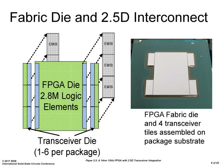
An Intel Slide from ISSCC, via PC Watch
Initially EMIB was thought of as a technology relating to Intel's acquisition of Altera and potential future embedded FPGA designs, and given the slide above and comments made at the Investor Day, it seems there are other plans for this technology too. The benefit of using multiple smaller dies over a large monolithic 600mm2 die is typically related to cost and yield, however the EMIB technology also has to be up to par and there may be a latency or compatibility trade-off.
Source: Intel, @TMFChipFool


124 Comments
View All Comments
doggface - Monday, February 13, 2017 - link
Your linked article has the conclusion that intel's fastest core-m is significantly faster. So it does nothing to bolster your argument, except to say it may be close but not in front, on an iPad vs MacBook.To then say. Well we don't have benchmarks but Apples stated improvements mean they are faster.. Needs citation.
Wilco1 - Saturday, February 11, 2017 - link
Eh? I guess you also still believe Atom is great and competitive? Intel shill?It's a well-known fact that current high-end phones outperform all low power SkyLake laptops and Chromebooks. Eg https://arstechnica.co.uk/gadgets/2017/02/samsung-... has the fastest Chromebook scoring 3230 on Geekbench 3. The current iPhone does 3567 (https://browser.primatelabs.com/geekbench3/8161439...
Now let's see what the A10X does...
Meteor2 - Sunday, February 12, 2017 - link
I thought people had figured out that synthetic benchmarks heavily dependent on single thread performance had little value? They're interesting, but they don't answer fundamental questions about performance across architectures and nodes.Until we see an Apple Ax chip running x265 or Agisoft photo scan or something else, you know, real, we can't make comparisons.
Wilco1 - Sunday, February 12, 2017 - link
Which of the subtests in Geekbench is synthetic exactly? http://www.geekbench.com/doc/geekbench4-cpu-worklo...I completely disagree we can't make any comparisons at all - benchmarks do give a pretty good idea what you can expect. Note video codecs and image processing say nothing about CPU performance given they are typically done by dedicated hardware or the GPU.
Single-threaded performance most definitely is quite fundamental. Multi-threaded performance is easy, remember most phones have at least 8 cores nowadays.
Meteor2 - Thursday, February 16, 2017 - link
Good link, I spent a while looking for that information but only found it for GB3.I still wouldn't rate those workloads as 'real' though, simply because they're canned tests, not actual workloads you might perform daily.
Meteor2 - Friday, February 10, 2017 - link
I never thought people would become fanboys of IC foundries, of all things.Not sure I should play along but... have you got any sources for your statements? For example, Apple on TSMC being competitive with Intel? I wasn't aware of any product overlap. It's a Core M inside a Mac Book, after all.
And TSMC 10 nm being used for an A10X? Er, no. As reported here, it's all being used for the Qualcomm 835 going into the Samsung S8 launching in April. What new Apple device is due to launch this side of September?
Meteor2 - Friday, February 10, 2017 - link
Oops, it's the Samsung foundries being used for the 835, not TSMC.name99 - Friday, February 10, 2017 - link
"Oops, it's the Samsung foundries being used for the 835, not TSMC." No shit...So your point is? TSMC have not stated that they're producing the A10X (of course not, they're not going to piss off their largest customer). What they HAVE said is that 10nm was in risk production last year, and is expected to deliver commercial products and TSMC revenue in Q1 this year.
There is also various circumstantial evidence (not to mention the historical pattern) that suggest what I've said, for example:
https://www.fool.com/investing/2016/09/22/your-fir...
Meteor2 - Sunday, February 12, 2017 - link
I thought you said one shouldn't listen to rumour sites.lefty2 - Friday, February 10, 2017 - link
Umm, this article doesn't really address the confusion about multiple architecures that seem the be released at the same time. If Intel's 8 gen core is on 14nm, what is 10nm Cannon lake? 9th gen? And what 8 gen core products are being released?