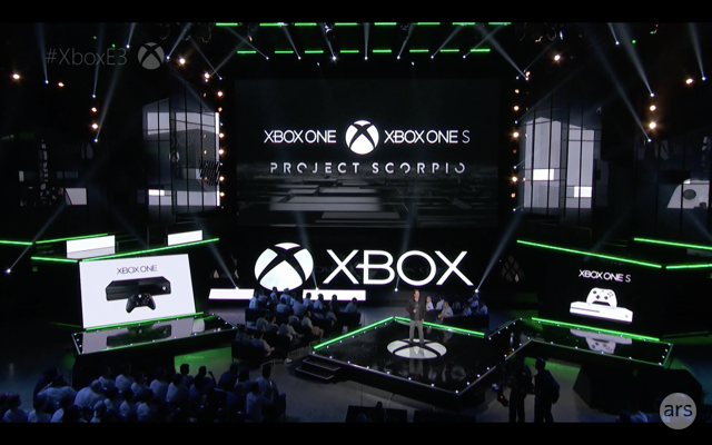
Microsoft Teases Project Scorpio for 2017: 8 cores, 6 TeraFLOPs, Backwards Compatible with Xbox. Zen or Jaguar?!
by Ian Cutress on June 13, 2016 2:02 PM EST- Posted in
- Microsoft
- Gaming
- Trade Shows
- Consoles
- E3

This news piece contains speculation, and suggests silicon implementation based on released products and roadmaps.The only elements confirmed for Project Scorpio are the eight cores, >6 TFLOPs, 320 GB/s, it's built by AMD, and it is coming in 2017. If anyone wants to officially correct any speculation, please get in touch.
Here’s an announcement at E3 for you. Microsoft just announced Project Scorpio, an internal project to develop the next generation Xbox set to be released in 2017. Project Scorpio is to be backwards compatible with Xbox One, and seems to be directly in line to compete with whatever Sony are supposedly releasing in the near future. But here’s some specifications for you that has my mind in a twist.
In the presentation, Microsoft states that the Project Scorpio SoC will have eight cores, up to 320 GB/s of memory bandwidth, and over 6 TeraFLOPs of power. To put this into context, this is more processing power than the recently announced AMD RX 480 GPU using a GCN 4 based architecture, set to be launched later this month. Microsoft specifically announced that Project Scorpio is to be launched next year, which puts a few things together worth mentioning.
By this time next year, we expect AMD’s Zen microarchitecture to be in full swing, and AMD has already showcased a silicon sample of an 8-core Zen processor. However, the current Xbox line relies on AMD’s ‘cat’ core architecture, which according to current AMD roadmaps doesn’t seem to feature anywhere for 2017. Without a direct confirmation, it’s hard to tell if Project Scorpio is the same Jaguar cores as the Xbox One, or the newer Zen microarchitecture. I would assume we won’t find out until later next year.
| Microsoft Console Specification Comparison | ||||||||||||||
| Xbox 360 | Xbox One | Project Scorpio | ||||||||||||
| CPU Cores/Threads | 3/6 | 8/8 | 8 / ? | |||||||||||
| CPU Frequency | 3.2GHz | 1.6GHz (est) | ? | |||||||||||
| CPU µArch | IBM PowerPC | AMD Jaguar | ? | |||||||||||
| Shared L2 Cache | 1MB | 2 x 2MB | ? | |||||||||||
| GPU Cores | 768 | ? | ||||||||||||
| Peak Shader Throughput | 0.24 TFLOPS | 1.23 TFLOPS | >6 TFLOPs | |||||||||||
| Embedded Memory | 10MB eDRAM | 32MB eSRAM | ? | |||||||||||
| Embedded Memory Bandwidth | 32GB/s | 102GB/s | ? | |||||||||||
| System Memory | 512MB 1400MHz GDDR3 | 8GB 2133MHz DDR3 | ? | |||||||||||
| System Memory Bus | 128-bits | 256-bits | ? | |||||||||||
| System Memory Bandwidth | 22.4 GB/s | 68.3 GB/s | 320 GB/s | |||||||||||
| Manufacturing Process | 28nm | ? | ||||||||||||
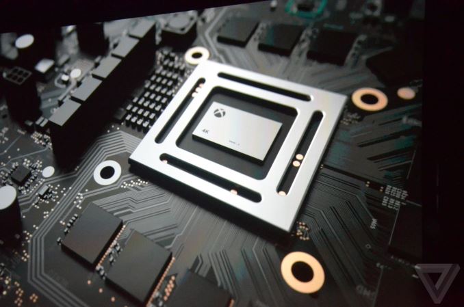
On the GPU side, the current Xbox One uses a 16 CU implementation in the SoC, with two disabled giving 14 CUs. We already know that AMD’s RX 480, running at 5 TFLOPs and built on Global Foundries 14nm FinFET process, runs in at 36 CUs. So Project Scorpio will have easily have more CUs than Xbox One, and judging by the shots in the video, the die size is relatively small. The Xbox One was built on TSMC’s 28nm HP process. At this point it’s still not confirmed if this is an AMD win, however judging by the comments towards backwards compatibility and SoC integration (where CPU and GPU are on the same silicon (or package)), all fingers would point in that direction.
| AMD Radeon GPU Specification Comparison | ||||||
| AMD Radeon RX 480 | AMD Radeon R9 390X | AMD Radeon R9 390 | AMD Radeon R9 380 | |||
| Stream Processors | 2304 (36 CUs) |
2816 (44 CUs) |
2560 (40 CUs) |
1792 (28 CUs) |
||
| Texture Units | (Many) | 176 | 160 | 112 | ||
| ROPs | (A Positive Integer) | 64 | 64 | 32 | ||
| TFLOPs (FMA) | >5 TFLOPs | 5.9 TFLOPs | 5.1 TFLOPs | 3.5 TFLOPs | ||
| Boost Clock | >1.08GHz | 1050MHz | 1000MHz | 970MHz | ||
| Memory Clock | 8Gbps GDDR5 | 5Gbps GDDR5 | 5Gbps GDDR5 | 5.5Gbps GDDR5 | ||
| Memory Bus Width | 256-bit | 512-bit | 512-bit | 256-bit | ||
| VRAM | 4GB/8GB | 8GB | 8GB | 2GB | ||
| Transistor Count | ? | 6.2B | 6.2B | 5.0B | ||
| Typical Board Power | 150W | 275W | 275W | 190W | ||
| Manufacturing Process | GloFo 14nm FinFET | TSMC 28nm | TSMC 28nm | TSMC 28nm | ||
| Architecture | GCN 4 | GCN 1.1 | GCN 1.1 | GCN 1.2 | ||
| GPU | Polaris 10? | Hawaii | Hawaii | Tonga | ||
| Launch Date | 06/29/16 | 06/18/15 | 06/18/15 | 06/18/15 | ||
| Launch Price | $199 | $429 | $329 | $199 | ||
The memory bandwidth of Project Scorpio, 320 GB/s, is also relatively interesting given the current rates of the RX 480 topping out at 256 GB/s. The 320 GB/s number seems round enough to be a GPU only figure, but given previous embedded memory designs is likely to include some form of embedded memory. How much is impossible to say at this point.
AMD has stated that the RX 480 is a VR Gaming capable card, so given what we've said about the Xbox One S tackling VR, it's clear that Project Scorpio is right on the money. AMD's business plan as of late is to expand its custom SoC business, and thus sticking Zen and a GCN 4 based architecture on a combined package or die for Microsoft makes a lot of sense. At the RX 480 announcement, it was stated that AMD wants to power the first 100 million VR users, and this would help towards that goal.
It's worth noting that this news piece contains a decent amount of speculation based on knowledge of the market, and the only elements confirmed for Project Scorpio are the eight cores, >6 TFLOPs, 320 GB/s, and it is coming in 2017. If anyone wants to officially correct any speculation, please get in touch.
Sources: Ars Technica (Carousel Image), Verge Live Blog (Video Screen Capture)
Additional: We can confirm that Scorpio will be an AMD based design, as expected.


101 Comments
View All Comments
Alexvrb - Tuesday, June 14, 2016 - link
Faster in terms of bandwidth, yes, but latency with GDDR5 is somewhat high. So there are technical hurdles if they really wanted to rip out the ESRAM. I don't think they will. The ESRAM will shrink VERY nicely on GloFo/Samsung's 14nm LPP process. They could bump speed up on it too - worst case scenario it truly is used as a large L4. An alternative is that they double down and make it faster and larger. Like 128MB of ESRAM. But I find that about as likely as them removing it entirely.Anyway, what's this talk of keeping Jaguar cores, Ian? If they continue to use a Cat core, they would use Puma+ with substantially higher clocks. 2.5+ would be well within the realm of possibility.
fallaha56 - Tuesday, June 14, 2016 - link
i'd be thinking 4 hyperthreaded Zen cores...killeak - Tuesday, June 14, 2016 - link
The ESRAM can only be used by the GPU, I don't think the latency matters much, considering that GPU are designed to deal with high latency. For GPUs, bandwidth is much more important.killeak - Tuesday, June 14, 2016 - link
Talking about the ESRAM on the XB1Fujikoma - Tuesday, June 14, 2016 - link
Wouldn't Scorpio just do an online update to the executable during install and bypass emulation for the most part. Maybe emulation if someone has a slow/limited internet connection.StevoLincolnite - Tuesday, June 14, 2016 - link
They could retain the eSRAM and use it as an L4 cache for the CPU and/or for retaining backwards compatibility.At 14nm I doubt the eSRAM is going to be taking up such a large % of the die-area.
patrickjp93 - Saturday, June 18, 2016 - link
No. ESRAM is just a cache. You can remove cache layers in a hierarchy and the CPU/GPU doesn't care. As long as there is system memory to pull from, you can disable every cache except L1 (because it has dedicated instruction and data lines and thus isn't like L2/L3/L4) and the CPU wouldn't notice.Alexvrb - Friday, July 22, 2016 - link
Sorry to post in an old thread but this is incorrect. First of all it's not just a cache. Second it's not about what the "CPU notices" but it's about what the code is attempting to utilize. XB1 games utilize that ESRAM directly and in some cases heavily to extract as much bandwidth as possible. Removing it would make backwards compatibility more difficult (though not impossible with emulation).Also: Killeak, the CPU can access ESRAM.
Eden-K121D - Tuesday, June 14, 2016 - link
I bet they will use GDDR5 X as it will allow for a smaller memory busImSpartacus - Monday, June 13, 2016 - link
Yeah, if that image is real, then it looks like there are 8 memory packages, which would be too many for a realistic HBM-based solution. So it's likely either GDDR5 or GDDR5X. Eight packages strongly suggests a 256-bit bus.And once you've got that bus width locked down, then you need the memory to run at an effective 10 Gbps if you want to get to 320 GB/s of bandwidth. It's convenient that GDDR5X is already available today at that speed.