Arm Unveils 2024 CPU Core Designs, Cortex X925, A725 and A520: Arm v9.2 Redefined For 3nm
by Gavin Bonshor on May 29, 2024 11:00 AM EST- Posted in
- CPUs
- Arm
- Smartphones
- Mobile
- SoCs
- Cortex
- 3nm
- Armv9.2
- Cortex-A520
- Cortex X925
- Cortex A725
Arm Cortex A725: Improvements to Middle Core Efficiency
The Arm Cortex-A725 is designed to balance performance and power efficiency, making it a critical component of the second-generation Armv9.2 architecture. Positioned as a mid-tier core, it complements the high-performance Cortex-X925 by offering robust capabilities for everyday computing tasks while maintaining energy efficiency. This core is especially targeted at devices that require consistent performance without the high power consumption associated with top-tier cores, such as smartphones, tablets, and laptops.
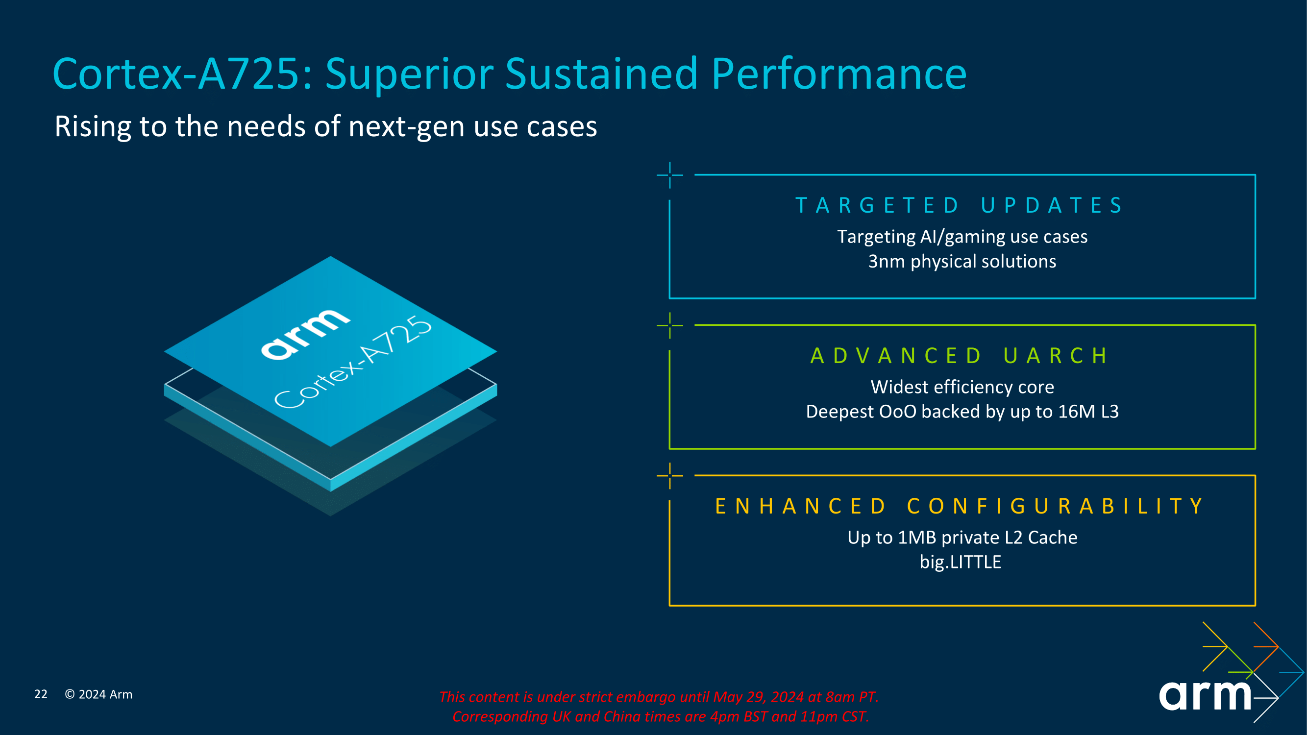
The Cortex-A725 builds on the successes of its predecessor, the Cortex-A720, with several key architectural enhancements. One of the significant improvements is the increased instruction issue queue and the expanded reorder buffer, which enable the core to handle more instructions simultaneously and execute them out of order for improved efficiency. This increase in the out-of-order execution window size allows the Cortex-A725 to utilize its execution units better, leading to smoother and faster processing of complex workloads.
The core also benefits from a new 1MB L2 cache configuration, which provides faster access to frequently used data and instructions. This larger cache size is designed to reduce latency and improve performance, particularly for applications that require rapid data retrieval. Additionally, the Cortex-A725 features enhancements in its register file structure, further streamlining data processing and reducing bottlenecks.
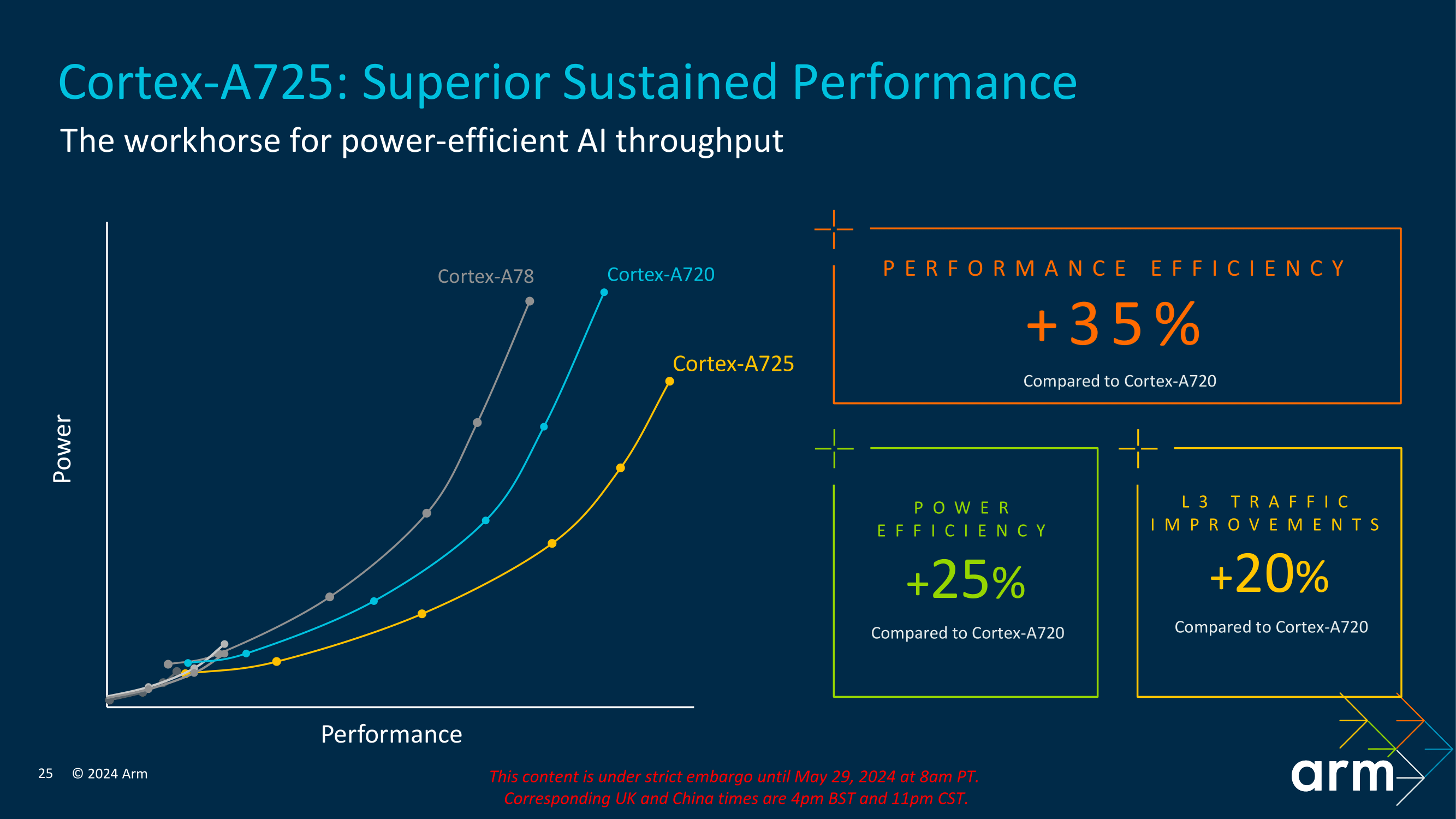
Power efficiency is a crucial aspect of the Cortex-A725's design. With leading-edge 2024 Cortex chips expected to be fabbed on newly-available 3nm process technologies from TSMC and others, the improved performance from these nodes is able to drive big improvements in energy efficiency, and Arm is leaning into that heavily with the A725. Overall, Arm is touting that A725 delivers significant power savings compared to previous generations. Compared to the Cortex-A720, the Cortex-A725 offers up to a 25% improvement in power efficiency (and 20% L3 traffic reduction), making it an ideal choice for mobile devices that require long battery life.
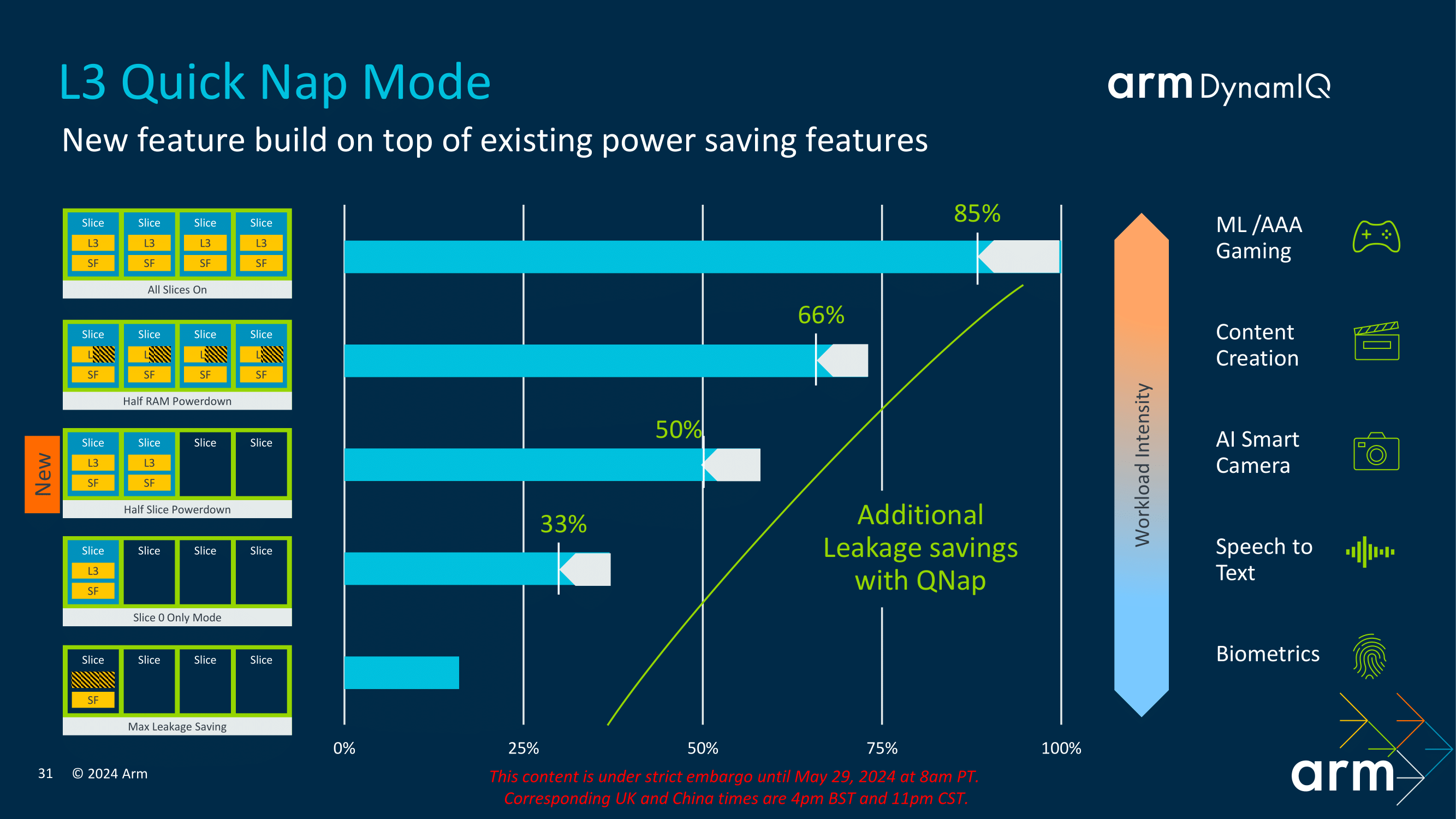
The core also features advanced power management capabilities, including dynamic voltage and frequency scaling (DVFS) and half-slice power-down modes. These features allow the Cortex-A725 to adjust its power consumption based on the current workload, ensuring energy is used efficiently without sacrificing performance.


55 Comments
View All Comments
SarahKerrigan - Wednesday, May 29, 2024 - link
"The core is built on Arm's latest 3 nm process technology, which enables it to achieve significant power savings compared to previous generations."ARM doesn't have lithography capabilities and this is a synthesizable core. This sentence doesn't mean anything.
meacupla - Wednesday, May 29, 2024 - link
AFAIK, the core design needs to be adapted to the smaller process node, and it's not as simple as shrinking an existing design.Ryan Smith - Wednesday, May 29, 2024 - link
Thanks. Reworded.dotjaz - Wednesday, May 29, 2024 - link
"ARM doesn't have lithography capabilities and this is a synthesizable core"And? Apple also doesn't have litho. You are telling me they can't implement anything with external foundries? Do you even know the basics of modern chip design? DTCO has been THE key to archieve better results for at least half a decade now.
Also this is clearly not just a synthesizable core. ARM explicitly announced this is avaiable as production ready cores, that means the implementations are tied to TSMC N3E and Samsung SF3 via DTCO, and this is the first time ARM has launched with ready for production hard core implementation.
You clearly didn't understand, and that's why it didn't mean anything TO YOU, and probably had to be dumbed down for you.
It actually makes perfect sense to me.
lmcd - Wednesday, May 29, 2024 - link
There was a turnaround time slide that didn't get Anandtech text to go with it that made this more clear, but a skim would miss it.zamroni - Monday, June 17, 2024 - link
it means the logic circuit is designed for 3nm's characteristics, e.g. signal latency, transistor density etc.older cortex designs can be manufactured using 3nm but it won't reach same performance as they were designed to cater higher signal latency of 4nm or older generations
Duncan Macdonald - Wednesday, May 29, 2024 - link
Lots of buzzwords but low on technical content. Much of this reads like a presentation designed to bamboozle senior management.Ryan Smith - Wednesday, May 29, 2024 - link
Similar sentiments were shared at the briefing.continuum - Thursday, May 30, 2024 - link
Whole tone of this article feels like it was written by an AI given how often (compared to what I'm used to in previous articles on this from Anandtech!) certain sentiments like "3nm process" and other buzzwords are used!name99 - Wednesday, May 29, 2024 - link
Not completely true...Interesting points (relative to Apple, I don't know enough about Nuvia internals to comment) include
- 4-wide load (vs Apple 3-wide load) is a nice tweak.
- 6-wide NEON is a big jump. Of course they have to scramble to cover that they STILL don't have SVE or SME; even so there is definitely some code that will like this, and the responses will be interesting. I can see a trajectory for how Apple improves SME and SSVE as a response, probably (we shall see...) also boosting NEON to 256b-SVE2. (But for this first round, still 4xNEON=2xSVE2)
Nuvia, less clear how they will counter.
Regardless I'm happy about both of these and requiring a response from Apple which, in turn, makes M a better chip for math/science/engineering (which is what I care about).
They're still relying on run-ahead for some fraction of their I-Prefetch. This SOUNDS good, but honestly, that's a superficial first response and you need to think deeper. Problem is that as far as prefetch goes, branches are of two forms – near branches (mostly if/else), which don't matter, a simple next line prefetcher covers them; and far branches (mostly call/return). You want to drive your prefetcher based on call/return patterns, not trying to run the if/else fetches enough cycles ahead of Decode. Apple gets this right with an I-prefetcher scheme that's based on call/return patterns (and has recently been boosted to use some TAGE-like ideas).
Ultimately it looks to me like they are boxed in by the fact that they need to look good on phones that are too cheap for a real NPU or a decent GPU. Which means they're blowing most of their extra budget on throughput functionality to handle CPU-based AI.
Probably not the optimal way to spend transistors as opposed to Apple or QC. BUT
with the great side-effect that it makes their core a lot nicer for STEM code! Maybe not what marketing wanted to push, but as I said, I'll take it as steering Apple and QC in the right direction.
I suspect this is part of why the announcement comes across as so light compared to the past few years – there simply isn't much new cool interesting stuff there, just a workmanlike (and probably appropriate) use of extra transistors to buy more throughput.