The Apple iPhone 6s and iPhone 6s Plus Review
by Ryan Smith & Joshua Ho on November 2, 2015 8:00 AM EST- Posted in
- Smartphones
- Apple
- Mobile
- SoCs
- iPhone 6s
- iPhone 6s Plus
Dual Sourcing A9: Two for the Price of Two
Perhaps more remarkable than the fact that the A9 is built using a FinFET process however is who it is being built by. For the first time Apple is dual sourcing the SoC – rather than using TSMC or Samsung exclusively, they are using both.
Broadly speaking, dual sourcing is a practice that has fallen out of style as the number of contract semiconductor manufacturers has dwindled and the cost of chip production has gone up. Because each manufacturer has its own rules and own best practices, to dual source a chip involves designing it twice, once for each manufacturer. This has made the cost of dual sourcing increase over time, and consequently dual sourcing falling out of fashion.
This of course is a big part of what makes Apple’s decision to dual source so unexpected. Apple is taking a much bigger gamble this time around by dual sourcing than they have on past SoCs where it was produced by a single manufacturer (be it TSMC or Samsung). Dual sourcing means that Apple’s costs to tape-out and bring-up A9 have very nearly doubled; they have to tape-out each version of the A9 for the respective fab’s rulesets, and then they have to go through the bring-up process with each in order to dial-in the yields and clockspeeds. They at least get to reuse the underlying architecture (e.g. Twister CPU and their PowerVR GPU), but actually creating a chip design for each fab is a significant part of the development costs for A9.
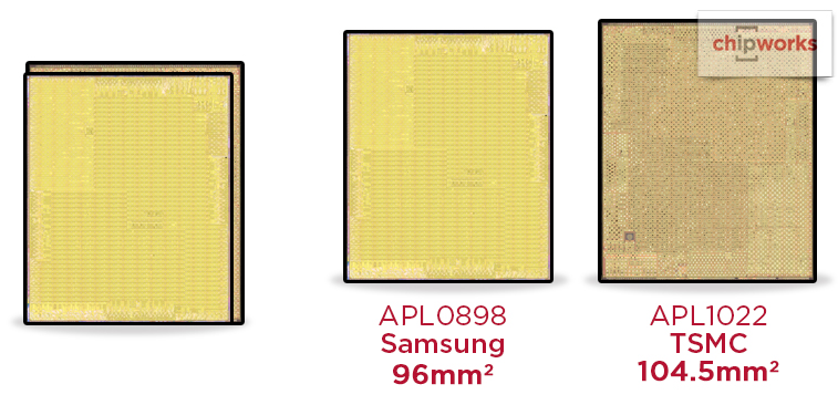
Samsung vs. TSMC A9 Die Size (Image Courtesy Chipworks)
The end result then is two similar but not quite equal chips that are produced by TSMC and Samsung respectively. Both are A9s, both feature the same CPU, GPU, memory interface, and all of the other bits that make up an A9. But each is produced at a different fab, according to the rules of that fab.
One of the immediate ramifications of dual sourcing is that the die sizes of the A9s are different. The A9 produced by Samsung on their 14nm FinFET Process is the smaller of the two, at 96mm2. Meanwhile the A9 produced on TSMC’s 16nm FinFET process is 104.5mm2, making it about 9% larger. Though not an immense difference in size (and not that we’d expect otherwise) there are tradeoffs to be had. With all other things held equal, the larger TSMC die would produce fewer complete dies per 300mm wafer, and any given die is more likely to have an imperfection since there are fewer dies for the same number of imperfections. This gives the Samsung A9 a slight edge in manufacturing thanks to its better density, however it’s equally important to note that in the real world there are a number of factors at play here, including manufacturing yields at each fab and how much each fab is charging Apple, so while the Samsung A9 is the smaller A9 it isn’t necessarily the cheaper A9.
The bigger question on many minds is whether there’s a performance difference between the two A9s. We wrote a bit on the subject a few weeks back, and the short answer is that it’s very difficult to tell. Due to chip quality being a distribution no two phones utilizing the same A9 are the same, and that means just comparing any two phones can’t tell us the whole story. Ultimately what one needs is a large number of phones to find the distribution, the median of that distribution, and how the medians compare. This is something that if done perfectly would require thousands of phones, and is really only possible for Apple or the competitive analysis teams at their well-funded competitors.
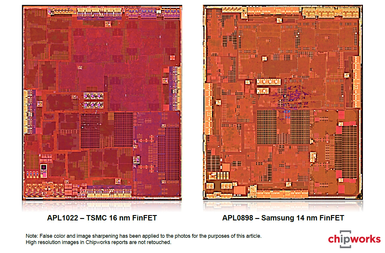
Apple A9 Die Shots (Image Courtesy Chipworks Teardown Report)
At this point then we don’t have anything new to add to the discussion – we don’t have enough data – though it is still a matter we are working on. Sometimes the best thing we can do is say is when we don’t have enough information, rather than extrapolating too much from too little information. I will note however that it’s ultimately in Apple’s best interests for the A9s to be as similar as possible, and there are steps they can take to ensure that, particularly in selecting which chips they will use.
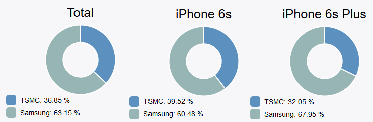
Current A9 Chip Manufacturer Distribution (Image Courtesy Hiraku)
Meanwhile looking at the data collected by iOS developer Hiraku’s CPU Identifier project, it’s interesting to note that of the 250K+ phones sampled so far, the Samsung A9 is in 63% of those phones, giving us a Samsung-to-TSMC ratio of nearly 2-to-1. This survey should not be considered the final word in the ratio between the two A9s since it can change over time and an opt-in survey of this fashion has an inherent self-selection bias, but with so many results it should be a reasonably accurate summary of the current situation.
What remains to be seen – and likely never to be answered outside the walls of One Infinite Loop – is why Apple dual sourced in the first place. We can certainly speculate on reasons they would do this – yield issues at a fab, a desire to avoid putting all of their eggs in one basket and giving one fab too much power, or even just wanting to ramp up A9 production quickly by doubling the number of fabs working on it. What is apparent however is that with Apple selling 48M iPhones in Q3’15 (note that the majority of these were not 6ses), A9 is a uniquely good candidate for dual sourcing. Apple sells enough iPhones that their large pile of cash aside they can absorb the cost of dual sourcing by spreading out the costs over tens of millions of high-margin chips, and if yields/supply were a factor in this decision then that’s all the more reason to dual source. This in turn makes me wonder if we’ll see Apple continue this strategy given their enormous volume, or if this was a one-time event due to the early nature of FinFET, leading to them settling on a single fab for the iPhone 7 launch.
Die Size: Hitting the Sweet Spot
Finally, before jumping into our discussion of the A9’s CPU and GPU, let’s talk about A9’s die size in a historical context. Unlike the transition from A7 to A8, Apple doesn’t get the advantage of a substantial transistor density improvement going from A8 to A9. To use TSMC as an example here (since they produced A8), their 16nm FinFET process is advertised as having 2x the density as their 28nm process, however compared to that same 28nm process their 20nm process had a 1.9x density advantage. In other words, the transition from 20nm HKMG planar to 16nm FinFET does not bring with it the same kind of density improvements we’ve seen in the last few generations.
In fact the only other time Apple has not had the advantage of a density improvement is the transition from A4 to A5, which saw Apple’s die sizes transition from what remains their smallest die to their largest die, all in a single generation. For A9 then Apple has to work smarter, as they can’t add a large number of transistors relative to A8 without ballooning A9’s die size outside of Apple’s sweet spot (and harming chip yields at the same time).
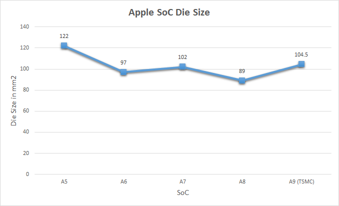
| Apple SoC Evolution | |||
| Die Size | Transistors | Process | |
| A5 | 122m2 | <1B | 45nm |
| A6 | 97mm2 | <1B | 32nm |
| A7 | 102mm2 | >1B | 28nm |
| A8 | 89mm2 | ~2B | 20nm |
| A9 | 96mm2/104.5mm2 | >2B | 14nm/16nm |
Consequently the A9s that we’re getting are surprisingly conservative. The TSMC A9 is 104.5mm2, some 17% larger than the TSMC A8. Meanwhile the Samsung A9 is the smaller of the two at 96mm2. The TSMC A9 is now Apple’s second-largest non-X SoC, but just barely so; it’s only 2.5mm2 larger than the A7. Otherwise with an average die size of 100mm2, this puts the A9 at the upper-bounds of Apple’s sweet spot.
Yet despite the limited gains in transistor density versus A8, Apple has managed to “bulk up” their SoC design by quite a bit. We’ll go over this in greater detail on the following pages, but of particular note is that Apple is now implementing what we believe to be a 6 core PowerVR GPU design, and Apple has significantly increased both the L2 and L3 cache sizes. Coupled with this is the jump to LPDDR4 (requiring more complex memory controllers) and numerous smaller improvements we’ll likely never learn about. The number of CPU cores remains unchanged at 2 however.
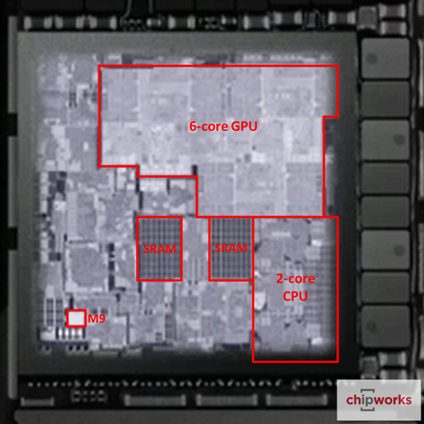
Chipworks' Initial Layout Analysis (Image Courtey Chipworks)

My Layout Analysis For A9 (Die Shot Courtesy Chipworks)
On a final note, now that we have die shots of both A9s from Chipworks, I must tip my hat towards Apple for releasing an accurate die shot of what we now know is the Samsung A9 in their iPhone 6s presentation. Up until now Apple has never released their own die shot of their SoCs, and in fact first-party die shots are becoming increasingly rare as a whole in the semiconductor industry. Consequently I had expected that Apple’s die shot was a fake, only to be far more impressed that it’s real. Furthermore despite the low resolution of the shot, Apple’s false color and contrast enhancements make it surprisingly clear where the CPU and GPU blocks are, and how many of each there are. This is a level of contrast that even the Chipworks shots can’t quite match this time around.


531 Comments
View All Comments
toukale - Monday, November 2, 2015 - link
Damn, "Now."Kevin G - Monday, November 2, 2015 - link
Not only is it enough to scare all other ARM SoC's but Intel has to be frighten by what Apple's engineers are capable of. Normalizing for clock speeds, it seems that the A9 is around Sandy/Ivy Bridge IPC and now with FinFET, there is a clock speed overlap with those chips as well. Intel has two newer generations of core designs (Haswell and Sky Lake) but they don't offer huge leaps over Sandy Bridge/Ivy Bridge. I'm really, really curious how the A9X in the iPad Pro will perform against various Core M designs in tablets. It is very conceivable that Apple could take the performance crown.Against low power i3/i5/i7 Sky Lake chips, Intel should still have performance lead. Granted those chips have a higher power budget it but it makes me wonder what Apple could pull off with a similar power budget.
As for the A9 itself, it is a very solid improvement and there is still room to grow. My personal prediction for the A9, SMT, appears to be absent. Considering the width of the A9 design, there should be some performance gains. Certainly while running in a 4T2C mode, power consumption will be higher, 2T1C should be lower power than 2T2C.
My predictions for the A10? I'm still sticking to the idea that SMT in Apple's CPU designs make sense so there is that. 4 MB of L2 cache and 12 MB of L3 cache are natural evolutions of their current topology. The GPU will core to an 8 core Rogue 7 design. The real SoC change will be in the memory subsystem with Apple adopting WideIO. I predict that the iPhone 7 will be the first product to drop the lightning connector and offer a USB Type-C port so USB and DisplayPort block will be included in the next iteration.
aliasfox - Monday, November 2, 2015 - link
While Intel should be worried about the performance Apple's SoC engineers are capable of, what they should really be worried about is price. Sure, Apple might only offer 75% of the performance of a ULV Core chip, but when it comes at 20-30% of the price, that's serious competition.Kevin G - Monday, November 2, 2015 - link
There is the whole dichotomy of Apple being an end product supplier with the iPhone/iPad vs. Intel being a parts supplier. There is also the difference that Apple needs a third party to manufacture the A9 chip where as Intel does this in house. Intel is more of a middle man here and thus inflates the end cost of the OEM handsets and tablets. Intel can make the same amount of profit if they were able to spur volume sales but that trade off has never appealed much to Intel who historically enjoyed healthy margins on component pricing.name99 - Monday, November 2, 2015 - link
Guys, it's time to stop this pretense that Apple is "almost" at Intel performance.Apple IPC has exceeded the best Intel has to offer by about 15%.
(gcc SPEC)
A9 vs haswell = 3148/1.85 / 4800/3.3 = 1.16
http://gcc.opensuse.org/SPEC/CINT/sb-czerny-head-6...
i5-4670T boost 3.3G ~4800
Or compare against the Broadwell in a MacBook:
https://browser.primatelabs.com/geekbench3/compare...
(Note that while the Bwell is nominally at 1.3GHz, Geekbench is short enough that it can turbo at 2.9GHz)
With the A7 Apple got an "inner" core that was equal to the best Intel has to offer. With the A9 they now have an uncore that matches Intel (look at all the memory dependent benchmarks in the Geekbench comparison above, things like Sobel, Sharpen, and FFT --- Apple now matches Intel pretty much exactly).
The only place where Apple still lags behind Intel (as far as the mobile space is concerned) is turbo-ing (ie an accurate on-SoC thermal model that allows parts of the SoC to run faster than rated up until the thermal budget is exceeded).
This does not necessarily mean that turbo is the feature Apple will implement next. There are other directions they could go which provide (in their opinion) a better tradeoff, at least for now, than turbo'ing. Possibilities include
- het core (add a low power low performance core. This sounds like big.LITTLE, but done right. The core selection and switching is done by a dedicated microcontroller which is tracking various CPU statistics like branch mispredictions and cache misses and using those to decide which core to use. The OS only sees one CPU; the het core is purely an internal implementation detail.
Done right papers suggest this can buy you about 20% power reduction.)
- KIP (kilo-instruction processor). A set of ideas that extend OoO from its current ability to tolerate latency out to L3, but not all the way to RAM, all the way out to RAM. This requires a ROB of size 1000 or so, and numerous modifications to allow the physical register set and load-store queues to match this size.
- post-rename loop buffer. Places the loop buffer not just after fetch, not just after decode, but all the way after rename. Requires various modifications (to handle the "frozen" renaming) but capable of a nice drop in power whenever executing out of the loop buffer.
Apart from starting down these paths, the obvious visible change for the A10 would appear to be that they
- drop 32-bit support (which should probably allow them to drop at least one pipeline stage, and simplify the decoder substantially)
- add support for the ARMv8.1a instructions.
SMT is (IMHO) a low priority for Apple. They can add more cores faster than they can design in SMT, and area won't be a critical constraint until the Moore's law scaling party stops.
vFunct - Monday, November 2, 2015 - link
They basically already have big.LITTLE with their M9 co-processor.doggface - Monday, November 2, 2015 - link
I'm sorry but no. Your geekbench scores mean nothing. Intel still has quite the lead. Otherwise Apple Mac book Pros would be using Apple SOCs.Apple will find that all the easy gains in CPU ipc/clocks are disappearing and like intel will struggle to make speed improvements beyond a certain level. Then chip cost will start going up. It is inevitable, it is physics.
All that aside. The A9 is impressive. Kudos to Apple.
IanHagen - Wednesday, November 4, 2015 - link
Whilst I agree mostly with you, the MacBook Pros don't sporting an Apple SoC is IMHO proof of nothing. The migration will be very costly and will brake compatibility with a ton of software. They can't simply slap a nice ARM chip on that thing and call it a day.DerekZ06 - Wednesday, November 4, 2015 - link
Switching architecture on the Mac book pros is like going from powerpc to x86 all over again.gonsolo - Tuesday, November 3, 2015 - link
Interesting. Can you quote some of the mentioned papers?