Qualcomm Details Hexagon 680 DSP in Snapdragon 820: Accelerated Imaging
by Joshua Ho on August 24, 2015 9:00 AM EST- Posted in
- Mobile
- Snapdragon
- Qualcomm
- SoCs
- Snapdragon 820
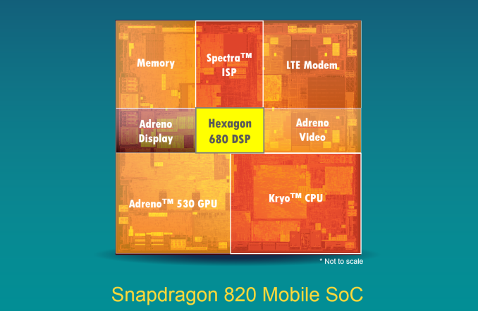
Although we tend not to focus too much on the tertiary aspects of a SoC, they are often important to enabling many aspects of the user experience. DSPs are important for a number of unique applications such as voice processing, audio processing, and other input processing applications. Before we get into the meat of the article though it's important to note that the above image is not a die shot or an actual block diagram, but is very roughly approximating the relative size of each component in the SoC.
Today at Hot Chips, Qualcomm elected to reveal a number of details about their Hexagon 680 DSP, which will ship in the Snapdragon 820. Those that have followed our coverage regarding the Snapdragon 820 ISP features will probably be able to guess that a number of features on the Snapdragon 820 Spectra ISP are enabled through the use of this newer DSP.
For those that are unfamiliar with DSPs, the basic idea behind DSPs is that they are a sort of in-between point in architecture design between highly efficient fixed function hardware (think: video decoders) and highly flexible CPUs. DSPs are programmable, but are rigid in design and are designed to do a limited number of tasks well, making them efficient at those tasks relative to a CPU, but more flexible than fixed function hardware. These design goals are typically manifested in DSPs as in-order architectures, which means that there's much less power and area dedicated on silicon to parallelize code on the fly. This means that while a DSP can do a number of workloads that would otherwise be impossible on a completely fixed-function block, you wouldn't want to try and use one to replace a CPU. It's important to emphasize that DSPs are generally more focused on instruction-level parallelism (single core performance) rather than thread-level parallelism (multi-core performance), so you won't see hundreds/thousands of "cores" in a DSP like you would in a GPU architecture like Maxwell.
Consequently the architecture of DSPs like the Hexagon 680 are relatively alien compared to standard CPUs, as optimization is everything in the applications where DSPs make sense. For example, DSP instruction sets are often VLIW (very long instruction word), in which multiple execution units are driven in parallel with a single instruction. Certain arithmetic operations are also highly accelerated with special instructions in order to enable key algorithms for signal processing such as Fast Fourier Transform (FFT).
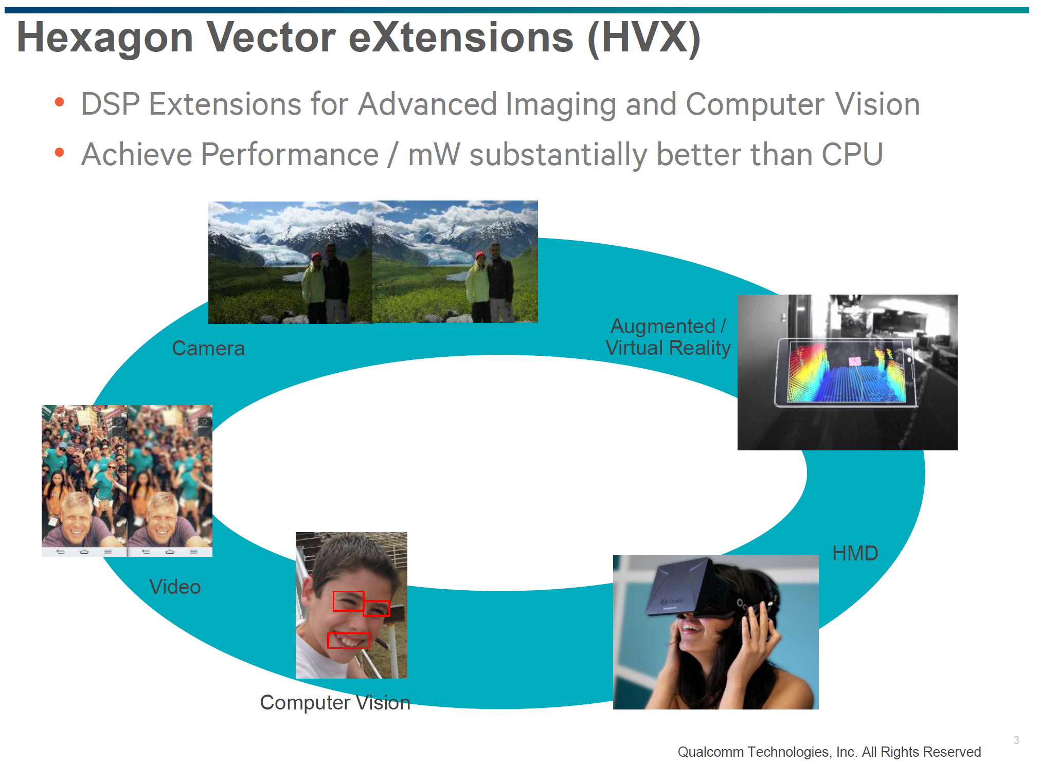
In the case of the Hexagon 680, one of the key features Qualcomm is focusing on for this launch are Hexagon Vector Extensions (HVX). HVX is designed to handle significant compute workloads for image processing applications such as virtual reality, augmented reality, image processing, video processing, and computer vision. This means that tasks that might otherwise be running on a relatively power hungry CPU or GPU can run a comparatively efficient DSP instead.

The HVX extension to Hexagon has 1024-bit vector data registers, with the ability to address up to four of these slots per instruction, which allows for up to 4096 bits per cycle. It's important to keep in mind that the instruction width is much smaller than this as this is a single instruction, multiple data (SIMD) unit which uses one operation over multiple chunks of data. There are 32 of these vector registers, which appear to be split between two HVX contexts. There is support for up to 32 bit fixed point decimal operations, but floating point is not supported to reduce die size and power consumption, as the previously mentioned applications for Hexagon 680 don’t need floating point support. As DSPs tend to have ISAs tailored for the application, the Hexagon 680 HVX units support sliding window filters, LUTs, and histogram acceleration at the ISA level. The performance of these units are said to be sufficient for 4K video post-processing, 20MP camera burst processing, and other applications with similar compute requirements.
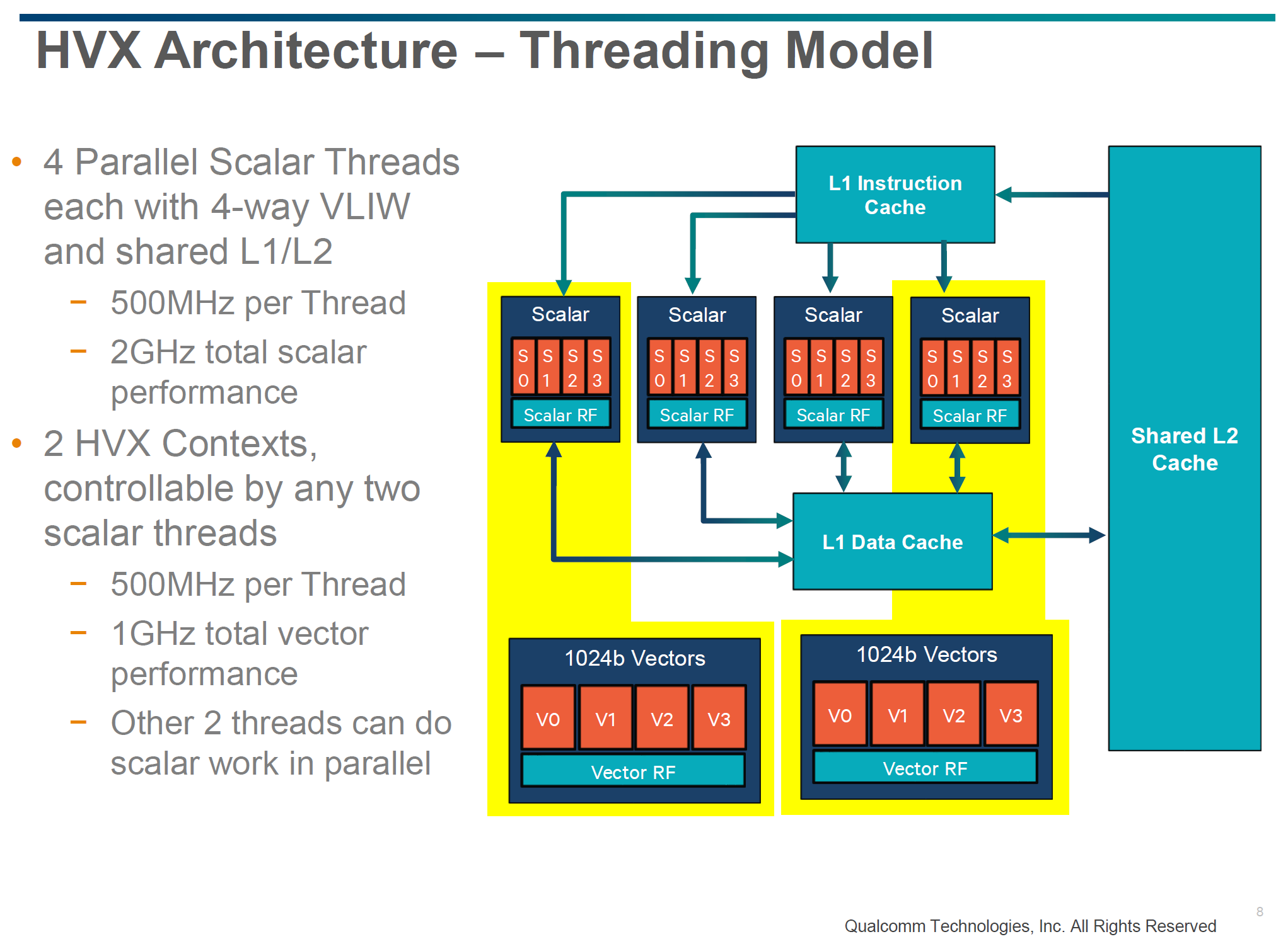

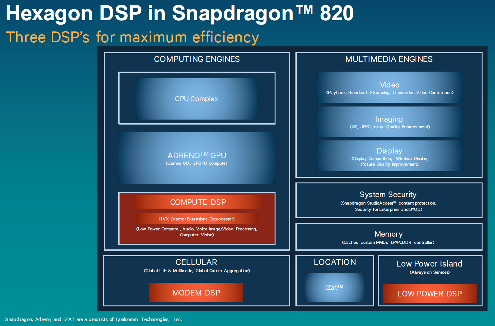
Outside of these details at a per-context basis, the threading model and memory hierarchy of the Hexagon 680 is quite unique. For scalar instructions, four threads are available with a 4-way VLIW architecture running at 500 MHz per thread. These scalar units all share an L1 instruction cache, L1 data cache, and L2 cache. The two HVX contexts in the Hexagon 680 can be controlled by any two scalar threads and also run at 500 MHz without stalling other scalar units not involved in controlling the vector units. This level of hardware-level multithreading along with QoS systems and L2 soft partitioning on a per-thread helps to make sure audio and imaging tasks aren’t fighting for execution time on the Hexagon DSP.
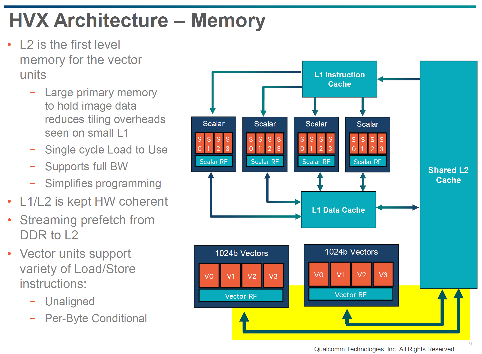
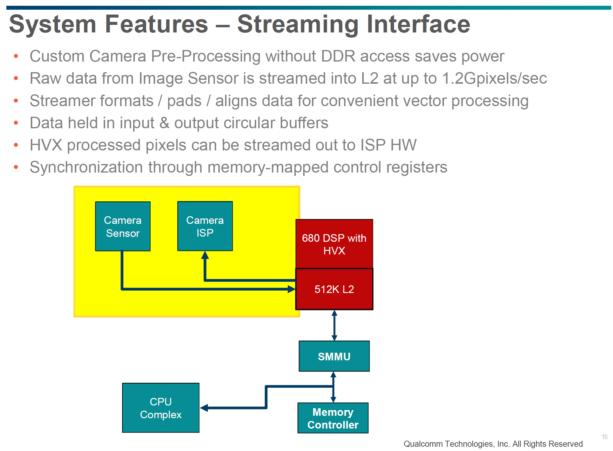
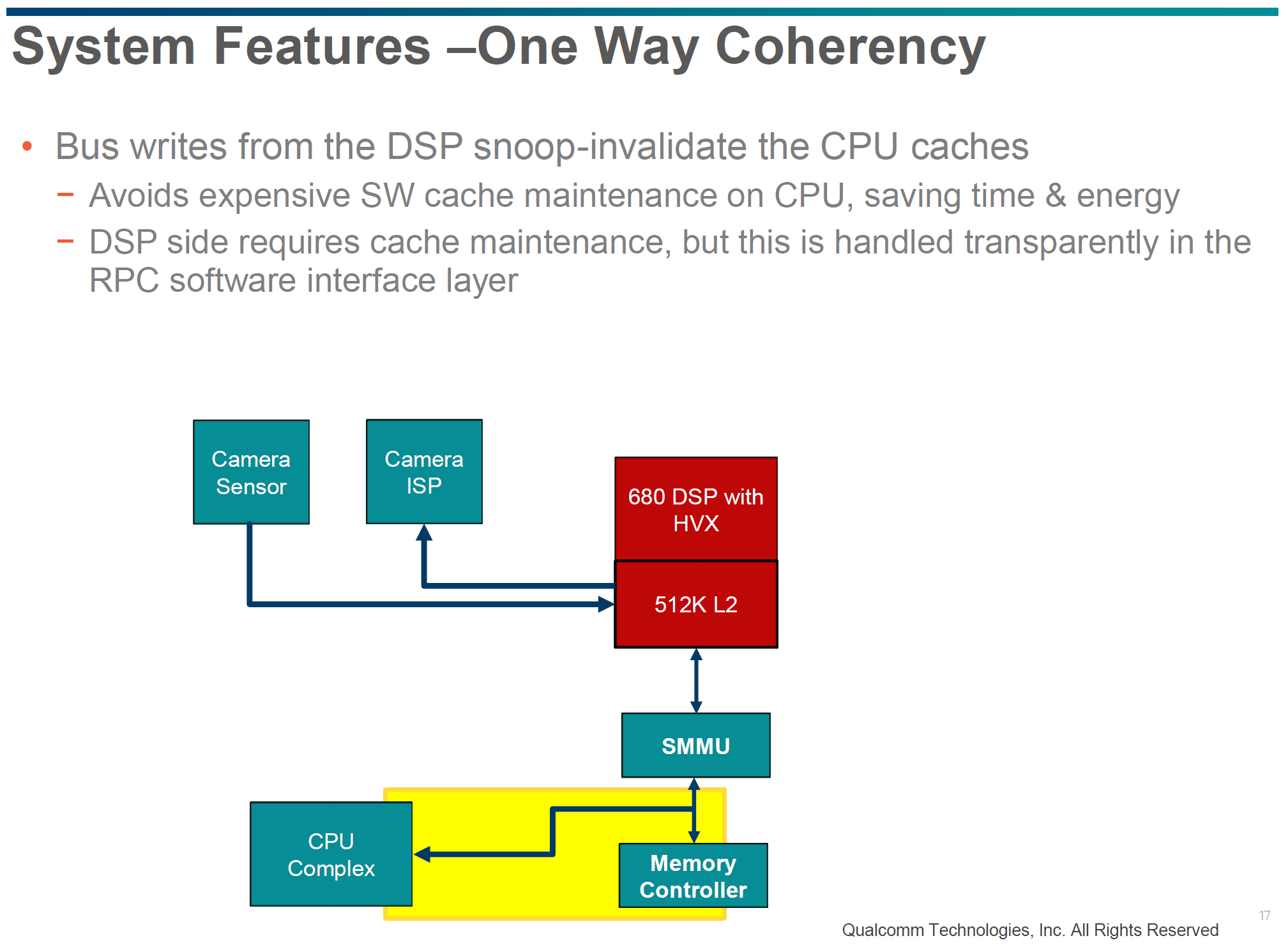
Meanwhile the vector units are fed exclusively from the L2 cache that is shared with the scalar units, a choice Qualcomm made due to the overhead that comes with an L1 cache for image processing workloads. This L2 cache can do load to use in a single cycle though, so one could argue that this is technically an L1 cache at times anyhow. The Hexagon 680 in the Snapdragon 820 will also be able to have data from the camera sensor directly streamed to the L2 cache and shared with the ISP to avoid the power cost of going off-die to DRAM. There’s also an SMMU (System Memory Management Unit) which allows for no-copy data sharing with the CPU for multiple simultaneous applications. DSP memory writes will also snoop-invalidate CPU cache without the need for the CPU to do any work involving cache maintenance to reduce power consumption and improve performance.

Relative to a quad-core Krait, the advantages of running some workloads on a DSP is enormous based on Qualcomm's internal benchmarks. According to Qualcomm, the NEON units in the Krait CPU are generally representative of NEON units within the industry, which is the reason why they've been used as the reference point here. Within a single logical “core”, Krait will only support 128-bit NEON with a single SIMD pipeline, compared to the 4-way, 1024-bit SIMD units of the Hexagon 680. SIMD threads also run on a 512KB L2-but-almost-L1 cache, as opposed to the 32KB L1 instruction/data cache of Krait, which helps to hide latency effects of DRAM. The NEON units of a Krait and many other ARM CPUs are capable of floating point, but in a workload like low light video enhancement Hexagon 680 will be able to complete the same amount of work at three times the speed, while using an order of magnitude less power due to the inherent advantages of a task-specific DSP architecture. The four scalar threads available in the DSP also means that entire algorithms can be off-loaded to the DSP instead of partially running on the CPU, which also reduces power consumption and makes it easier for developers to take advantage of the DSP.


While Hexagon 680’s vector and scalar engines are useful for heavy-duty signal processing workloads, the addition of the low power island (LPI) DSP makes it possible to do away with separate sensor hubs in smartphones. According to Qualcomm, this DSP is completely separate from the scalar and vector compute DSP previously discussed (yet still part of the overall Hexagon DSP design), and sits on its own power island so the rest of the SoC can be shut down while keeping the LPI on. This also shouldn’t have a different process technology or a radically different standard cell library, as the advantages from the leading edge FinFET process should help significantly with power consumption.
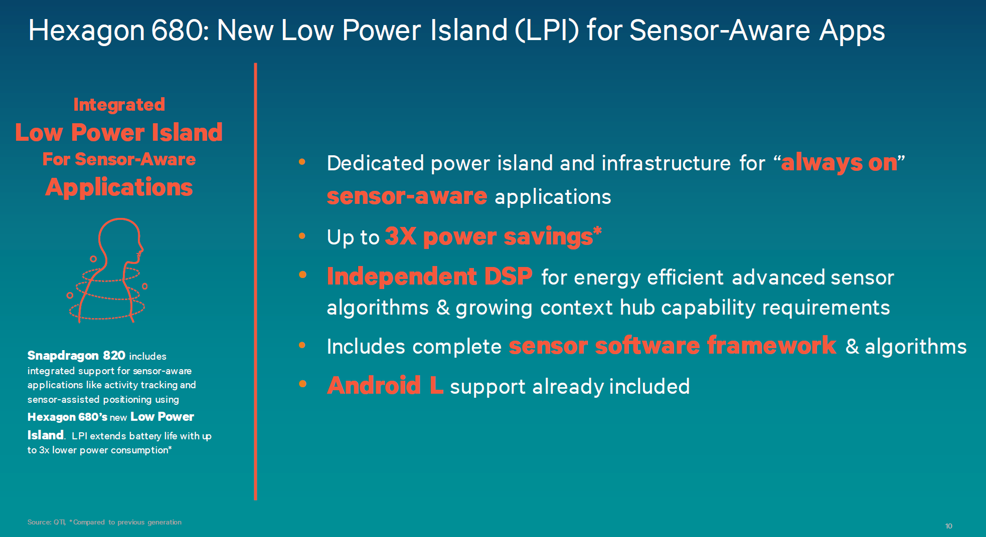
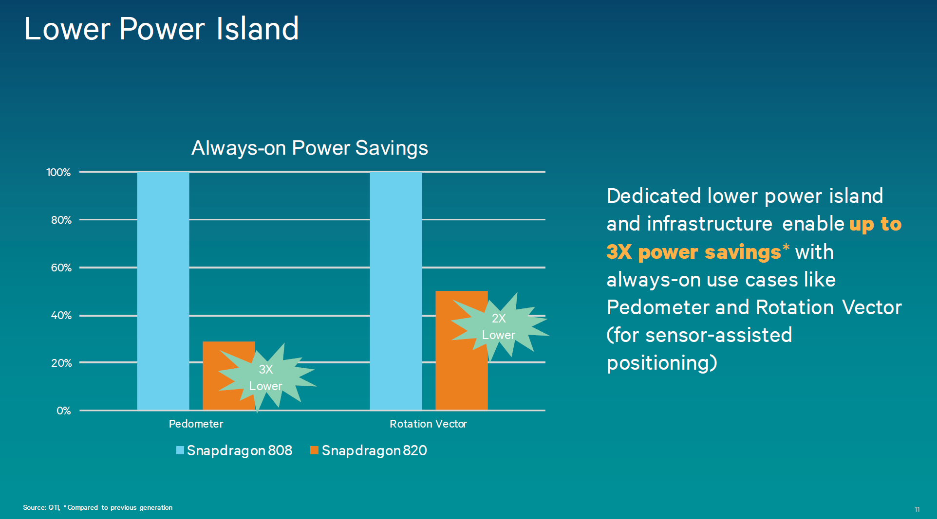
It’s said that this low power island with an independent DSP and newer process node is enough to improve power efficiency by up to three times in certain workloads compared to Snapdragon 808. I suspect that this was done instead of a comparison to the MSM8974/Snapdragon 800 generation because the Hexagon DSP was updated in the move from Snapdragon 805 to 808. Qualcomm emphasized the choice of a DSP over an MCU for this task, as in their internal testing a DSP delivers better power efficiency than a Cortex M-class MCU for more advanced sensor algorithms. The software stack for all of these features is already said to be quite complete, with a framework and algorithms included for OEM development. The broader Hexagon 600 series SDK is also quite extensive, with a number of utilities to allow for faster and easier development.
If you’re like me, after going through all of this information you might be wondering what the value of these vector DSP extensions are. In discussions with Qualcomm, it seems that the reasoning behind pushing a number of image processing tasks to the Hexagon DSP core is mostly because the algorithms behind things such as HDR video, HDR image merging, low light image enhancement, and other advanced algorithms are still in flux even from software update to software update. As a result, it isn’t viable to make these aspects of the imaging pipeline done in fixed-function hardware. Without the use of the Hexagon DSP, these tasks could potentially end up running on the CPU or GPU, affecting user experience in the form of higher shot to shot latency, reduced battery life when using the camera, and higher skin temperatures. It remains to be seen whether OEMs using Snapdragon 820 will use these DSPs to the fullest extent, but the Snapdragon 820 is shaping up to be a promising 2016 high-end SoC.


41 Comments
View All Comments
name99 - Monday, August 24, 2015 - link
What you're saying is substantially silly. Apple provides a large library of a variety of different types of image processing operations (including user provided filters) in Core Image; and these are implemented on the GPU on both OSX and iOS, apparently very fast and at low power.Apple may well at some point put a DSP onto the A- chips (especially once the QC-supplied LLVM framework I described above is mature, and perhaps also once Swift is a little more mature), but their doesn't seem to have been a compelling argument so far, since the A4 at least.
There's also the issue that, while the argument I gave re memory access regularity is correct, there is the problem that insisting on a fixed-point only path is problematic. While a few algorithms easily match a fixed-point pathway (basically linear filters), as soon as you include any sort of non-linear processing you have to spend a whole lot of time constantly normalizing. If Apple were to include a DSP for upcoming areas of interest (like perceptrons for machine learning), they'd probably make it FP all the way (maybe 16bit FP, but still FP) rather than bother with a fixed point setup.
MrSpadge - Monday, August 24, 2015 - link
He was not talking about the PCIe latency, but about the instruction latency. I.e. the time it takes for instructions to complete. It's huge on GPUs. That's how they achieve their efficiency for massively parallel tasks. But it hurts them badly for any other tasks (branches).And "it has more power" means nothing in the mobile world if the alternative has "enough" computing power and completes the task for (significantly) less energy. Also being flexible is nice, but no real advantage is the alternative can do the job well.
saratoga4 - Monday, August 24, 2015 - link
^^^ Exactly. Latency on GPUs is very high, and that has nothing to do with PCIe.Its fine that you can take a 200 watt desktop GPU and run basic tasks like filtering with good performance, but you're still using a 200 watt GPU to do something that a DSP could do for orders of magnitude lower power consumption, which is one reason why GPUs are almost never used for image processing on mobile devices. You'll kill the battery. The other main reason being that inability of GPUs to handle high branching and non-parallel image processing tasks.
ddriver - Monday, August 24, 2015 - link
What do you mean by "very high". Microseconds, nanoseconds, milliseconds? Is it too high to be useful? I've gotten GPU compute to run on a millisecond resolution, and it could probably go even lower, now do tell, for what kind of tasks is ONE THOUSANDTH of a second too slow?I've seen such arguments before, from people who "heard that GPU compute is unusable for audio processing because latency is too high" - few weeks later I had an audio engine processing offline audio at 20 times the rate, at which the CPU was capable of, and I haven't heard that argument since then. And that wasn't the best part, the CPU was pretty much sitting idle, giving it much more clocks to handle real time audio at a lower latency.
Image processing is in its nature a parallel task. But please, do tell at least several more times how GPUs can't handle branching, because I feel like the several times that was already mentioned are really not enough.
The figures for that DSP are on average twice as fast as the CPU at 8 times less power. Given that the GPU can easily outperform the CPU in parallel tasks at least 10 times EASY, at a comparable power envelope, I'd say it is about as efficient as the DSP, with the advantages of having more throughput, more features and more portable when it comes to programming it.
Last but not least, with OpenCL 2's SVM, believe it or not, but GPUs massively outperform CPUs even for stuff like binary tree search, which is in its nature a non parallel workload. So there is that too...
saratoga4 - Monday, August 24, 2015 - link
>Image processing is in its nature a parallel task.haha yeah sure all image processing algorithms are parallel by their nature. If you really believe that I think we're unlikely to be able to discuss much of anything. Congrats on learning OpenCL though. I think you're letting it go to your head a bit though.
name99 - Monday, August 24, 2015 - link
"which is one reason why GPUs are almost never used for image processing on mobile devices"I just told you GPUs ARE used for lotsa image processing on iOS.
The reason they aren't used on Android probably has to do with lack of a decent framework, and no standard hardware model for Google to target.
name99 - Monday, August 24, 2015 - link
"whereas with the DSP you must explicitly target it, and that code will do you no good on other platforms."This is not exactly true. QC have contributed to LLVM a framework (currently in flux) for designating different pieces of code to run on different ISAs, along with the tools (bundling and linking) necessary for this to happen. The vision is that you write your app in a more-or-less constrained version of C (and presumably soon C++, maybe even Swift), annotate certain functions and memory blocks by their target ISA, and everything else just happens automatically.
Like everything it will take time to fully fall into place, but there is a scheme there that has general potential for anyone interested in accelerators, whether GPUs, DSPs, or more specialized devices.
As for GPU vs DSP, I'd say the difference is in how much irregularity the device expects. GPUs have to expect a lot of memory irregularity, and thus provide a lot of transistors to cope with that fact. DSPs target much more regular memory access, and don't have to spend those transistors and their related power costs. Of course this assumes all things being equal, and if 10x the money and resources are spent on GPU design, optimization, and compilers, then things will not be equal...
extide - Monday, August 24, 2015 - link
The DSP is actually TINY in die area, probably smaller than a single A53 core, for example. The picture in this article is just a logical representation, NOT an accurate floorplan at all.extide - Monday, August 24, 2015 - link
EDIT Sorry meant smaller than single A57 -- not A53 :)ddriver - Monday, August 24, 2015 - link
I doubt that, as they claim it is faster than a quad core CPU's SIMDs, as efficient as the DSP may be, it is neither magic nor a miracle. This performance cannot come from nowhere. IIRC the DSP benefit is that instructions do a lot more work, but it still takes transistors to do all that work, regardless of how many instructions it takes.