Tick Tock On The Rocks: Intel Delays 10nm, Adds 3rd Gen 14nm Core Product "Kaby Lake"
by Brett Howse & Ryan Smith on July 16, 2015 10:15 AM EST
For almost as long as this website has been existence, there has been ample speculation and concern over the future of Moore’s Law. The observation, penned by Intel’s co-founded Gordon Moore, has to date correctly predicted the driving force behind the rapid growth of the electronics industry, with massive increases in transistor counts enabling faster and faster processors over the generations.
The heart of Moore’s Law, that transistor counts will continue to increase, is for the foreseeable future still alive and well, with plans for transistors reaching out to 7nm and beyond. However in the interim there is greater concern over whether the pace of Moore’s Law is sustainable and whether fabs can continue to develop smaller processes every two years as they have for so many years in the past.
The challenge facing semiconductor fabs is that the complexity of the task – consistently etching into silicon at smaller and smaller scales – increases with every new node, and trivial physics issues at larger nodes have become serious issues at smaller nodes. This in turn continues to drive up the costs of developing the next generation of semiconductor fabs, and even that is predicated on the physics issues being resolved in a timely manner. No other industry is tasked with breaking the laws of physics every two years, and over the years the semiconductor industry has been increasingly whittled down as firms have been pushed out by the technical and financial hurdles in keeping up with the traditional front-runners.
The biggest front runner in turn is of course Intel, who has for many years now been at the forefront of semiconductor development, and by-and-large the bellwether for the semiconductor fabrication industry as a whole. So when Intel speaks up on the challenges they face, others listen, and this was definitely the case for yesterday’s Intel earnings announcement.
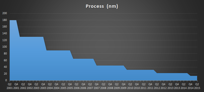
As part of their call, Intel has announced that they have pushed back their schedule for the deployment of their 10nm process, and in turn it has affected their product development roadmap. Acknowledging that the traditional two year cadence has become (at best) a two and a half year cadence for Intel, the company’s 10nm process, originally scheduled to go into volume production in late 2016, is now scheduled to reach volume production in the second half of 2017, a delay of near a year. This delay means that Intel’s current 14nm node will in effect become a three year node for the company, with 10nm not entering volume production until almost three years after 14nm hit the same point in 2014.

Intel’s initial struggles with 14nm have been well publicized, with the company having launched their 14nm process later than they would have liked. With their 22nm process having launched in Q2 of 2012, 14nm didn’t reach the same point until Q4 of 2014, and by traditional desktop standards the delay has been even longer. Ultimately Intel was hoping that the delays they experienced with 14nm would be an aberration, but that has not been the case.
Intel’s latest delay ends up being part of a larger trend in semiconductor manufacturing, which has seen the most recent nodes stick around much longer than before. Intel’s leading node for desktop processors in particular has been 22nm for close to three years. Meanwhile competitors TSMC and Samsung have made much greater use of their 28nm nodes than expected, as their planar 20nm nodes have seen relatively little usage due to leakage, causing some customers to wait for their respective 16nm/14nm FinFET nodes, which offer better electrical characteristics at these small geometries than planar transistors. Observationally then there’s nothing new from Intel’s announcement that we haven’t already seen, but it confirms the expected and all too unfortunate news that even the industry’s current bellwether isn’t going to be able to keep up with a traditional two year cadence.
Intel Historical Development Cadence
Meanwhile the fact that 14nm is going to be around for another year at Intel presents its own challenges for Intel’s product groups as well as their fabrication groups, which brings us to the second part of Intel’s announcement. Intel’s traditional development model for processors over the last decade has been the company’s famous tick-tock model – releasing processors built on an existing architecture and a new manufacturing node (tick), and then following that up with a new architecture built on the then-mature manufacturing node (tock), and repeating the cycle all over again – which in turn is built on the two year development cadence. Intel wants to have new products every year, and alternating architectures and manufacturing nodes was the sanest, safest way to achieve that. However with the delay of 10nm, it means that Intel now has an additional year to fill in their product lineup, and that means tick-tock is on the rocks.
Previously rumored and now confirmed by Intel, the company will be developing a 3rd generation 14nm Core product, to fit in between the company’s forthcoming 14nm Skylake (2015) and 10nm Cannonlake (2017) processor families.
| Intel Core Family Roadmap | ||||
| Previous Roadmap | New Roadmap | |||
| 2014 | Broadwell | Broadwell | ||
| 2015 | Skylake | Skylake | ||
| 2016 | Cannonlake | Kaby Lake (New) | ||
| 2017 | (10nm New Architecture) | Cannonlake | ||
| 2018 | N/A | (10nm New Architecture) | ||
The new processor family is being dubbed Kaby Lake. It will be based on the preceding Skylake micro-architecture but with key performance enhancements to differentiate it from Skylake and to offer a further generation of performance improvements in light of the delay of Intel’s 10nm process. Intel hasn’t gone into detail at this time over just what those enhancements will be for Kaby Lake, though we are curious over just how far in advance Intel has been planning for the new family. Intel has several options here, including back-porting some of their planned Cannonlake enhancements, or looking at smaller-scale alternatives, depending on just how long Kaby Lake has been under development.
Kaby Lake in turn comes from Intel’s desire to have yearly product updates, but also to meet customer demands for predictable product updates. The PC industry as a whole is still strongly tethered to yearly hardware cycles, which puts OEMs in a tight spot if they don’t have anything new to sell. Intel has already partially gone down this route once with the Haswell Refresh processors for 2014, which served to cover the 14nm delay, and Kaby Lake in turn is a more thorough take on the process.
Finally, looking at a longer term perspective, while Intel won’t be able to maintain their two year development cadence for 10nm, the company hasn’t given up on it entirely. The company is still hoping for a two year cadence for the shift from 10nm to 7nm, which ideally would see 7nm hit volume production in 2019. Given the longer timeframes Intel has required for both 14nm and 10nm, a two year cadence for 7nm is definitely questionable at this time, though not impossible.
For the moment at least this means tick-tock isn’t quite dead at Intel – it’s merely on the rocks. What happens from here may more than anything else depend on the state of the long in development Extreme Ultra-Violet (EUV) technology, which Intel isn’t implementing for 10nm, but if it’s ready for 7nm would speed up the development process. Ultimately with any luck we should hear about the final fate of tick-tock as early as the end of 2016, when Intel has a better idea of when their 7nm process will be ready.
Source: Intel Earnings Call via Seeking Alpha (Transcript)


138 Comments
View All Comments
Alketi - Thursday, July 16, 2015 - link
Quantum computing isn't the answer, as it'll be targeted at math problems that gain an advantage by trying all possibilities at once. It won't run normal software.But, yes, new technologies or approaches are needed, because Moore's Law is about to hit a brick wall. We're quickly headed toward single-digit numbers of electrons between the source and drain, which won't be sustainable and obviously has a finite limit.
EdgeOfDetroit - Thursday, July 16, 2015 - link
I never understood the logic of going down to 14nm from 22nm. That's a much bigger % decrease than going from 28nm to 22nm. At the time I thought "well if they can do it, more power to them". But now its clear they actually couldn't do it. They should have gone to something like 17nm to keep the % decrease to not be completely crazy. I guess we're probably getting 10nm sooner than we otherwise would, but it has delayed everything else in the mean time.zepi - Thursday, July 16, 2015 - link
Intel never did 28nm, they had 32nm process by their definitions before.nevcairiel - Thursday, July 16, 2015 - link
The use of FinFETs made the extra shrink possible, so, why not? :)nandnandnand - Thursday, July 16, 2015 - link
No. 28nm is a half node for wimps.The real shift was from 32nm to 22nm to 14nm, which is about the same proportional decrease each time.
Intel is still in the lead and the 3rd generation of 14nm will give them time to make architectural improvements. Like those 28nm AMD and NVIDIA GPUs that have been around forever. Moore's law may be dead but sitting and waiting for extreme ultraviolet lithography before taking on 10nm, 7nm and less is a good strategy.
Notmyusualid - Thursday, July 16, 2015 - link
+1extide - Thursday, July 16, 2015 - link
Nobody went from 28 -> 22Intel 45 -> 32 -> 22 -> 14 -> 10
TSMC 50 -> 40 -> 28 -> 20 -> 16FF (20nm BEOL) -> 16FF+ (16nm BEOL)
3DoubleD - Thursday, July 16, 2015 - link
It is because the numbers 22 and 14 are somewhat arbitrary. There are in fact no actual dimensions that correspond with these numbers anymore. The node measurements are something of a historical nomenclature that has lost all real meaning. The actual improvements in density are not directly reflected by the node number, they are just a name.The delays are inevitable based on the increasing complexity of lithography, etching, and metal layers. This doesn't even account the increasing troubles modeling channel behavior that contain only a few dopant atoms and all the problems that come along with having short channels.
Progress does not end here though, the harder shrinking silicon becomes, the sooner Intel and others will shift to the next paradigm of ICs, which according to the ITRS roadmap will likely be InGaAs channels and then perhaps InAs-Si tunnel FETs. Should be an exciting decade to come.
Nagorak - Friday, July 17, 2015 - link
"Should be an exciting decade to come."Well this decade sure has been boring. I'm honestly not expecting more from the next either. Even if Intel is still shrinking nodes, CPU performance has been almost stagnant for 5 years now. The die shrinks aren't helping unlock much performance at this point and on the desktop side you'll never save enough power to recoup the cost of buying a new more energy efficient processor.
Death666Angel - Thursday, July 16, 2015 - link
Intel never had a 28nm node. It went from 45nm -> 32nm -> 22nm -> 14nm.