Tick Tock On The Rocks: Intel Delays 10nm, Adds 3rd Gen 14nm Core Product "Kaby Lake"
by Brett Howse & Ryan Smith on July 16, 2015 10:15 AM EST
For almost as long as this website has been existence, there has been ample speculation and concern over the future of Moore’s Law. The observation, penned by Intel’s co-founded Gordon Moore, has to date correctly predicted the driving force behind the rapid growth of the electronics industry, with massive increases in transistor counts enabling faster and faster processors over the generations.
The heart of Moore’s Law, that transistor counts will continue to increase, is for the foreseeable future still alive and well, with plans for transistors reaching out to 7nm and beyond. However in the interim there is greater concern over whether the pace of Moore’s Law is sustainable and whether fabs can continue to develop smaller processes every two years as they have for so many years in the past.
The challenge facing semiconductor fabs is that the complexity of the task – consistently etching into silicon at smaller and smaller scales – increases with every new node, and trivial physics issues at larger nodes have become serious issues at smaller nodes. This in turn continues to drive up the costs of developing the next generation of semiconductor fabs, and even that is predicated on the physics issues being resolved in a timely manner. No other industry is tasked with breaking the laws of physics every two years, and over the years the semiconductor industry has been increasingly whittled down as firms have been pushed out by the technical and financial hurdles in keeping up with the traditional front-runners.
The biggest front runner in turn is of course Intel, who has for many years now been at the forefront of semiconductor development, and by-and-large the bellwether for the semiconductor fabrication industry as a whole. So when Intel speaks up on the challenges they face, others listen, and this was definitely the case for yesterday’s Intel earnings announcement.
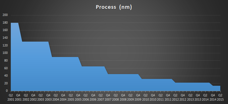
As part of their call, Intel has announced that they have pushed back their schedule for the deployment of their 10nm process, and in turn it has affected their product development roadmap. Acknowledging that the traditional two year cadence has become (at best) a two and a half year cadence for Intel, the company’s 10nm process, originally scheduled to go into volume production in late 2016, is now scheduled to reach volume production in the second half of 2017, a delay of near a year. This delay means that Intel’s current 14nm node will in effect become a three year node for the company, with 10nm not entering volume production until almost three years after 14nm hit the same point in 2014.

Intel’s initial struggles with 14nm have been well publicized, with the company having launched their 14nm process later than they would have liked. With their 22nm process having launched in Q2 of 2012, 14nm didn’t reach the same point until Q4 of 2014, and by traditional desktop standards the delay has been even longer. Ultimately Intel was hoping that the delays they experienced with 14nm would be an aberration, but that has not been the case.
Intel’s latest delay ends up being part of a larger trend in semiconductor manufacturing, which has seen the most recent nodes stick around much longer than before. Intel’s leading node for desktop processors in particular has been 22nm for close to three years. Meanwhile competitors TSMC and Samsung have made much greater use of their 28nm nodes than expected, as their planar 20nm nodes have seen relatively little usage due to leakage, causing some customers to wait for their respective 16nm/14nm FinFET nodes, which offer better electrical characteristics at these small geometries than planar transistors. Observationally then there’s nothing new from Intel’s announcement that we haven’t already seen, but it confirms the expected and all too unfortunate news that even the industry’s current bellwether isn’t going to be able to keep up with a traditional two year cadence.
Intel Historical Development Cadence
Meanwhile the fact that 14nm is going to be around for another year at Intel presents its own challenges for Intel’s product groups as well as their fabrication groups, which brings us to the second part of Intel’s announcement. Intel’s traditional development model for processors over the last decade has been the company’s famous tick-tock model – releasing processors built on an existing architecture and a new manufacturing node (tick), and then following that up with a new architecture built on the then-mature manufacturing node (tock), and repeating the cycle all over again – which in turn is built on the two year development cadence. Intel wants to have new products every year, and alternating architectures and manufacturing nodes was the sanest, safest way to achieve that. However with the delay of 10nm, it means that Intel now has an additional year to fill in their product lineup, and that means tick-tock is on the rocks.
Previously rumored and now confirmed by Intel, the company will be developing a 3rd generation 14nm Core product, to fit in between the company’s forthcoming 14nm Skylake (2015) and 10nm Cannonlake (2017) processor families.
| Intel Core Family Roadmap | ||||
| Previous Roadmap | New Roadmap | |||
| 2014 | Broadwell | Broadwell | ||
| 2015 | Skylake | Skylake | ||
| 2016 | Cannonlake | Kaby Lake (New) | ||
| 2017 | (10nm New Architecture) | Cannonlake | ||
| 2018 | N/A | (10nm New Architecture) | ||
The new processor family is being dubbed Kaby Lake. It will be based on the preceding Skylake micro-architecture but with key performance enhancements to differentiate it from Skylake and to offer a further generation of performance improvements in light of the delay of Intel’s 10nm process. Intel hasn’t gone into detail at this time over just what those enhancements will be for Kaby Lake, though we are curious over just how far in advance Intel has been planning for the new family. Intel has several options here, including back-porting some of their planned Cannonlake enhancements, or looking at smaller-scale alternatives, depending on just how long Kaby Lake has been under development.
Kaby Lake in turn comes from Intel’s desire to have yearly product updates, but also to meet customer demands for predictable product updates. The PC industry as a whole is still strongly tethered to yearly hardware cycles, which puts OEMs in a tight spot if they don’t have anything new to sell. Intel has already partially gone down this route once with the Haswell Refresh processors for 2014, which served to cover the 14nm delay, and Kaby Lake in turn is a more thorough take on the process.
Finally, looking at a longer term perspective, while Intel won’t be able to maintain their two year development cadence for 10nm, the company hasn’t given up on it entirely. The company is still hoping for a two year cadence for the shift from 10nm to 7nm, which ideally would see 7nm hit volume production in 2019. Given the longer timeframes Intel has required for both 14nm and 10nm, a two year cadence for 7nm is definitely questionable at this time, though not impossible.
For the moment at least this means tick-tock isn’t quite dead at Intel – it’s merely on the rocks. What happens from here may more than anything else depend on the state of the long in development Extreme Ultra-Violet (EUV) technology, which Intel isn’t implementing for 10nm, but if it’s ready for 7nm would speed up the development process. Ultimately with any luck we should hear about the final fate of tick-tock as early as the end of 2016, when Intel has a better idea of when their 7nm process will be ready.
Source: Intel Earnings Call via Seeking Alpha (Transcript)


138 Comments
View All Comments
boeush - Sunday, July 19, 2015 - link
I think you're conflating interest vs. product positioning. The 'enthusiast' offerings cost an arm and a leg, because they are limited runs and high margin products. Were they mass-produced and (relatively) cheap, hell yea there'd be much wider interest.Additionally, even those enthusiast parts presently feature the same mobile-optimized core designs - not ones designed from the ground-up for performance as a first priority. Intel's present design rule that any feature costing an extra 1% in power must yield at least 2% more performance, is fine for mobile and data center products, but is antithetical to desktop/workstation products. Which is why the latter us a market in decline currently - it's being cannibalized by mobile, and no surprise: it's a self fulfilling prophesy by design.
AnnonymousCoward - Tuesday, July 21, 2015 - link
Agreed. Cut the iGPU nonsense.txjr88 - Thursday, July 16, 2015 - link
Regarding Igpu, I wonder is they could use the gpu space and put down copper layers for heatsink/heat conductor. I realize the chip size has to be the same for heat surface area concerns, but why not have heat conductors either layered or embedded into the actual die space. Intel needs to think outside the box and go for what end users really want not the penny pinching customers who are essentially middle men these days. Speed sells, iGPU not so much.boeush - Thursday, July 16, 2015 - link
As far as layering heat spreading layers, I think graphene is the material of choice. Forget about making circuits/transistors with it for the near future; use it for its unmatched heat conductance instead. With graphene/silicon layered sandwich construction, it may even become possible to layer multiple CPUs on top of each other (in a 3D stack) for huge core counts per die. Would make Xeon Phi look like a toy. How would you like 128 Skylake Y cores on a single chip?txjr88 - Friday, July 17, 2015 - link
My thought was to use existing technology now. Graphene brings EPA health issues/concerns and material compatibility/material handling issues while copper use in now with existing processes/machines.boeush - Friday, July 17, 2015 - link
??? What health issues? You do realize that any time you use a pencil on paper, you are smearing graphene flakes over cellulose fibers? As far as material compatibility and handling, I thought IBM demonstrated graphene film growth on silicon carbide, like 5 years ago? Not knocking the practicality of copper, but to get good heat pipe performance you'd need to lay it on pretty thick. Not so with graphene. Hell, even spraying on a layer of carbon nanotubes would probably make for a better heat pipe....txjr88 - Monday, July 20, 2015 - link
Go to EPA website and learn. In making chips, you don't spray stuff and glop it on by hand. The existing machines/processes are extremely fine tuned and any new material is a huge major big deal.boeush - Tuesday, July 21, 2015 - link
Learn what? If graphene had any appreciable toxicity, we'd have to urgently reclassify all graphite-lead pencils as toxic waste. As for material application, spraying, spin coating, CVD, annealing - whatever it takes. But no, not by hand...Aspiring Techie - Friday, July 17, 2015 - link
The only problem with that would be heat dissipation. Each core would have to be clocked extremely low so that not much heat is generated. The crippled single core performance would most likely outweigh the gain in parallelization.boeush - Friday, July 17, 2015 - link
Perhaps, to a degree... But the whole idea of inserting heat spreader layers between cores is to suck the heat away toward the perimeter of the 'sandwich', where it would presumably be transferred to some sort of a heatsink/cooler. Can't argue real numbers since nobody (that I know of) had tried it before, and I'm not skilled/knowledgeable/equipped enough to realistically simulate it - but it would be worth a try IMHO.