Understanding Qualcomm's Snapdragon 810: Performance Preview
by Joshua Ho & Andrei Frumusanu on February 12, 2015 9:00 AM EST- Posted in
- SoCs
- Qualcomm
- Mobile
- Gobi
- Snapdragon 810
While we can dance around the issue, it’s impossible to have any real discussion about Snapdragon 810 without addressing the flurry of rumors that have surrounded this SoC. There have been rumors of overheating, delays, and all sorts of defects. In light of this, the Snapdragon 810 and its performance has been the subject of intense interest. In order to learn more, we recently met with Qualcomm to do a deep dive on the Snapdragon 810 and properly benchmark it for comparison against other SoCs.
While those that have followed the SoC market closely are likely to be quite familiar with the Snapdragon 810, it’s still worth going over the basics of the SoC before diving into aspects such as performance. In general, the area of greatest focus and one of the most important aspects of any SoC is the application processor. In the case of the Snapdragon 810, Qualcomm has licensed ARM’s Cortex A57 and A53 architectures for the CPU, which we’ve previously discussed in depth in our review of the Galaxy Note 4 Exynos. The Snapdragon 810 comes with the A57 cluster clocked at 1958 MHz and the A53 cluster at 1555 MHz.
| Qualcomm Snapdragon S810 Specifications | |||
| SoC | Snapdragon 810 | Snapdragon 805 | Samsung Exynos 5433 |
| CPU | 4x Cortex A53@1.555GHz 4x Cortex A57 r1p1 @1.958GHz 2MB L2 cache |
4x Krait 450@2.65GHz 4x512KB L2 cache |
4x Cortex A53 r0p1@1.3GHz 512KB L2 cache 4x Cortex A57 r1p0 @1.9GHz 2MB L2 cache |
| Memory Controller |
2x 32-bit @ 1555MHz LPDDR4 24.8GB/s b/w |
4x 32-bit @ 800MHz LPDDR3 25.6GB/s b/w |
2x 32-bit @ 825MHz LPDDR3 13.2GB/s b/w |
| GPU | Adreno 430 @ 600MHz |
Adreno 420 @ 600MHz |
Mali T760MP6 @ 700MHz |
| Mfc. Process |
TSMC 20nm SoC |
TSMC 28nm HPm |
Samsung 20nm HKMG |
For the most part, Qualcomm seems to have adopted a relatively similar approach by using a 4+4 big.LITTLE design, which means that four Cortex A57s serve as the “high power” cores, and four Cortex A53s work as the “low power” cores, with a CCI-400 to allow for cache coherency between the two clusters. However, while the architecture is licensed from ARM the actual implementation of the logic has been optimized by Qualcomm to improve performance and/or power consumption. Like most recent big.LITTLE SoCs, Qualcomm’s Snapdragon 810 has all eight cores exposed to applications, and relies upon task scheduling mechanisms to decide how to place threads on each core. However Qualcomm, as opposed to all other licensees of big.LITTLE, has decided to stray away from ARM's and Linaro's software implementation, and we'll be scratching the surface of what this means in terms of power and performance on the Snapdragon 810.
Outside of the SoC, Qualcomm has integrated an Adreno 430 GPU, which is said to deliver a performance improvement of 30%, possibly more for a shader-heavy workload. Outside of this the Adreno GPUs continue to be a black box in terms of technical detail. Qualcomm states that this GPU wasn’t a straight extension of the Adreno 420 which suggests that there have been architectural changes to the GPU, although we weren’t told what they were. We should be seeing final clocks running at 600MHz, meaning the GPU is running at the same frequency as the Adreno 420 in Snapdragon 805 devices.

To feed these components and the rest of the SoC, Qualcomm has fitted the SoC with a dual-channel 32-bit (total 64-bit) wide LPDDR4-1555 memory interface, which means a peak of 24.9 GB/s in memory bandwidth and basically maintains parity with the Snapdragon 805 despite the reduced bus width. The move to LPDDR4 should also bring a reduction in power consumption of the memory interface of up to 20% when compared to LPDDR3.
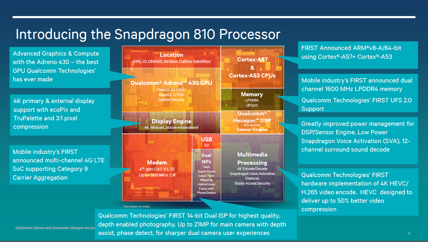
Outside of the GPU and CPU, Qualcomm has focused on iterating all other aspects of this SoC. The Snapdragon 810 represents Qualcomm’s first high-end SoC with an HEVC encoder, which is said to support up to 4K30 although we were not told the exact bit rate limits or any other encoder settings. Along the same lines, Qualcomm has upgraded the ISP in the Snapdragon 810 to a “14-bit” dual ISP, which allows for features such as multiple cameras for depth mapping or other computational photography features. This new ISP in the Snapdragon 810 can process 1.2 GP/s, in contrast with the 1 GP/s of the Snapdragon 805’s ISP. As mentioned in previous articles, this ISP is clocked at 600 MHz. The audio codec is the WCD9330 which is carried over from the Snapdragon 805.
On the RF side of things, Qualcomm is introducing a new category 9 modem that is built into the Snapdragon 810. In our experience, an integrated modem does improve battery life, although in practice these benefits will likely be difficult to distinguish from a multitude of other factors on total battery life. While one might guess that this is similar to the MDM9x45 external modem, it seems that there may not be enough bandwidth to support both upload and 3x download carrier aggregation. We also see a new suite of RF360 parts to accompany the Snapdragon 810, which include an antenna tuner, CMOS PA/antenna switch, and envelope tracker. Outside of the WTR3925 transceiver that was introduced with the Snapdragon 805, we see a new WTR3905 companion chip for 3x download CA and upload CA. In addition, we see a new variant of the QCA6174 WiFi chip, the QCA6174A, which enables MU-MIMO and a separate chip to enable 802.11ad.
RF
The basics can be all that's necessary to cover the RF changes in the Snapdragon 810 platform, but now is as good a time as any to really get down to the details of how this all works. For a while now, RF has been a black box. We’ve done some work on demystifying some aspects of RF, but there’s still quite a bit left to cover. While we have covered parts of RF systems like the envelope tracker, that’s only one piece of the puzzle. As a front-end solution, we’re still missing a great deal of nuance on the CMOS PA and integrated switch, along with the dynamic antenna tuner. In addition, there’s quite a bit in the pipeline that has come out since our last article on the state of Qualcomm’s RF components. WTR3925 and MDM9x35 have been shipping in mobile devices for a while, and we’re on the cusp of seeing new modems like Qualcomm’s MDM9x45 so there’s no better time to talk about all of this.
For those that are unfamiliar with how radio works at a high level it’s well worth going over in order to understand how everything comes together. At the basic level, on the receive path we can start at the antenna. The antenna is rather simple, and its goal is to convert radio waves into electrical energy. There’s definitely a lot more to this area, but for now that’s really all the knowledge that’s necessary. From there, the next step in the path is an antenna switch, which is used to select the right path for receive and transmit depending on the band used. A duplexer is the next step in the chain and is used to allow transmit and receive to be split into two separate parts. Before we get to the transceiver itself, filters (ideally) strip out any received signal that is out of the desired frequency band.
Once we get to the transceiver, a low noise amplifier takes the relatively weak signal from the filter and boosts it. After this, a down-converter converts the frequency of the signal to a baseband frequency by using a local oscillator that generates a signal that is mixed with the incoming signal. This is necessary because the signal is coming in at anywhere from 700 MHz to 5 GHz, which is almost impossible to process in real time with a relatively low-clocked DSP. In addition, this makes it easier to reject noise and due to the conversion in frequency it’s much easier to design an amplifier for this signal. That’s exactly what happens after this down-conversion. The signal is then split into the in-phase and quadrature components to make signal processing simpler. Another amplifier boosts the signal and then it reaches the baseband. At the baseband, an analog to digital converter processes the signal, and then the signal is demodulated. Once this is accomplished, the rest of the system simply sees the information as if it were packets of data in a format like TCP/IP.
The path for transmission is similar, although there are a few modifications on that end. Starting from the baseband, the information is modulated into a specific format, then converted from a digital signal to an analog one as it leaves the baseband. From here, the signal travels through another set of amplifiers before it is combined and raised to the frequency needed for transmission in the up-converter. At this point, another driver amplifier is used to amplify the signal before it leaves the transceiver. There’s currently not much need to understand what the driver amplifier does other than to know that it exists, so don’t worry about that for now. What’s definitely important is the power amplifier. This is the point where the signal is driven from the relatively low levels in the transceiver and baseband to high enough power to contact a cell tower. After this is done, the signal goes through the duplexer, through an antenna switch, out to the antenna.
At a high level, that’s how things work. To break things down into the simplest form, there are two distinct sections. The RF front end and baseband. The front end is designed to accurately capture as much information from the antennas as possible and filter it down to a form that the baseband can handle. The baseband is where all information is processed after the front end and receiver, and acts as the control center for rest of the RF system. It’s definitely a lot to take in, but it will help a lot with understanding the relevance of RF360, WTR3925, and MDM9x35.


119 Comments
View All Comments
Uplink10 - Friday, February 13, 2015 - link
That price is too high and is not intended for manufacturers, Bay Trail chips also have a high price but for the price of Bay Trail chip you get motherboard with Bay Trail chip. Also that chip is an overkill for a tablet, with that much features (vPro-remote bios...) it should be used as a server.metayoshi - Friday, February 13, 2015 - link
The price on that website IS for manufacturers:Recommended Customer Price (RCP) is pricing guidance only for Intel products. Prices are for direct Intel customers, typically represent 1,000-unit purchase quantities, and are subject to change without notice. Prices may vary for other package types and shipment quantities. Listing of RCP does not constitute a formal pricing offer from Intel.
Taneli - Thursday, February 12, 2015 - link
K1 is tablets only with no integrated modem and X1 is closer to 10w TDP so it needs active cooling. The Snapdragon here is a totally different chip. And Apple doesn't sell SOCsdragonsqrrl - Thursday, February 12, 2015 - link
Errr... what? 10W TDP? Link please?kron123456789 - Friday, February 13, 2015 - link
Well, Nvidia claimed that Tegra X1 consumes 10W while running The Elemental demo.jjj - Thursday, February 12, 2015 - link
Funny how you insist in comparing it to the 805 not the 5433 when commenting on the Geekbench results. That kind of behavior shows the desire to please the maker of the product not to inform the users, yet it is a persistent Anandtech problem.Might have missed it but you don't seem to even mention clocks either , the SD 810 is at 2GHz i assume and the Exynos is at 1.9GHz, 5% is plenty. Nothing on throttling ,nothing on power, you basically help them better their damaged image without having the complete data. That's unethical and you just accept being manipulated into it.
As for overheating ,we don't know what clocks they targeted and i haven't noticed any mention of what revision you are testing. For delays,there are already delays (that's not debatable) compared to their most optimistic previously disclosed timing.
Just showing the perf numbers we already knew,without looking beyond that doesn't really help.
A5 - Thursday, February 12, 2015 - link
I really doubt Qualcomm was going to let them take apart their reference tablet to get power numbers.That said, 2015 seems like a good "skip year" on the Android flagship front unless the Exynos 7420 is a real blockbuster. I don't really see anything in this article that supports the conclusion at the end.
TylerGrunter - Thursday, February 12, 2015 - link
I fully support you there. Snapdragon 810 seems to be competitive with Exynos 5433 and A8 chips, the sad news is that those are 6 month old and there are not the SoCs it will have to compete with.Exynos 7420 has been a beast in preliminary benchmarks, so I hope for that (or Intel coming with something) not to have what you are calling a "skip year".
And for tablets we'll always have Intel or NVidia.
JimRamK - Thursday, February 12, 2015 - link
What about Intel chips?A5 - Thursday, February 12, 2015 - link
AFAIK, they don't have any design wins in phones. I don't think 14nm is going to change that, but we'll see.