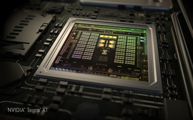
NVIDIA Tegra X1 Preview & Architecture Analysis
by Joshua Ho & Ryan Smith on January 5, 2015 1:00 AM EST- Posted in
- SoCs
- Arm
- Project Denver
- Mobile
- 20nm
- GPUs
- Tablets
- NVIDIA
- Cortex A57
- Tegra X1
In the past few years, we’ve seen NVIDIA shift their mobile strategy dramatically with time. With Tegra 2 and 3, we saw multiple design wins in the smartphone space, along with the tablet space. These SoCs often had dedicated GPUs that were quite unlike what we saw in NVIDIA’s desktop and laptop GPUs, with a reduced feature set and unique architecture. However, with Tegra K1 we saw a distinct shift in NVIDIA’s SoC strategy, as the Tegra K1 was the first mobile SoC to achieve parity in GPU architecture with desktop GPUs. In the case of the Tegra K1, this meant a single Kepler SMX which made for truly incredible GPU performance. However, in the time since we’ve seen companies like Apple release new SoCs such as the A8X, which managed to bring largely similar performance with less power.
NVIDIA of course is never content to stay idle for too long and let themselves be surpassed, which has led to the company developing their Tegra SoCs on a roughly yearly cadence. In NVIDIA’s development timeline, 2014 brought us the Tegra K1-32, the company’s first SoC to integrate a modern high-performance GPU architecture (Kepler), and later on the TK1-64, a K1 with NVIDIA’s own in-house developed ARMv8 Denver CPU in place of the 32bit ARM A15 CPU.
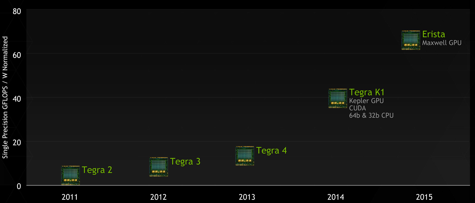
NVIDIA's GTC 2014 Tegra Roadmap
2014 also brought a revision to NVIDIA’s public Tegra roadmap: for 2015 NVIDIA would bump the previously announced Parker SoC and release a new in its place, Erista. This schedule change ended up being quite a surprise due to the fact that NVIDIA had up until this time released their roadmaps roughly 2 years out, whereas Erista was put on the map less than a year before it was to be announced. More unusual, NVIDIA offered up minimal details of Erista; it would be powered by a Maxwell GPU with no additional information on the CPU or manufacturing process. Parker on the other hand – NVIDIA’s planned Denver + Maxwell + 16nm FinFet part – fell off the schedule, with NVIDIA not officially canceling it but also saying little else about it.
Now in 2015 and with the launch of the Tegra X1, we can finally begin putting the picture together. Erista as it turns out is something of a rapid release product for NVIDIA; what had been plans to produce a 16nm FF part in 2015 became plans to produce a 20nm part, with Erista to be that part. To pull together Erista NVIDIA would go for a quick time-to-market approach in SoC design, pairing up a Maxwell GPU with ARM Cortex A57 & A53 GPUs, to be produced on TSMC’s 20nm SoC process.
CPU
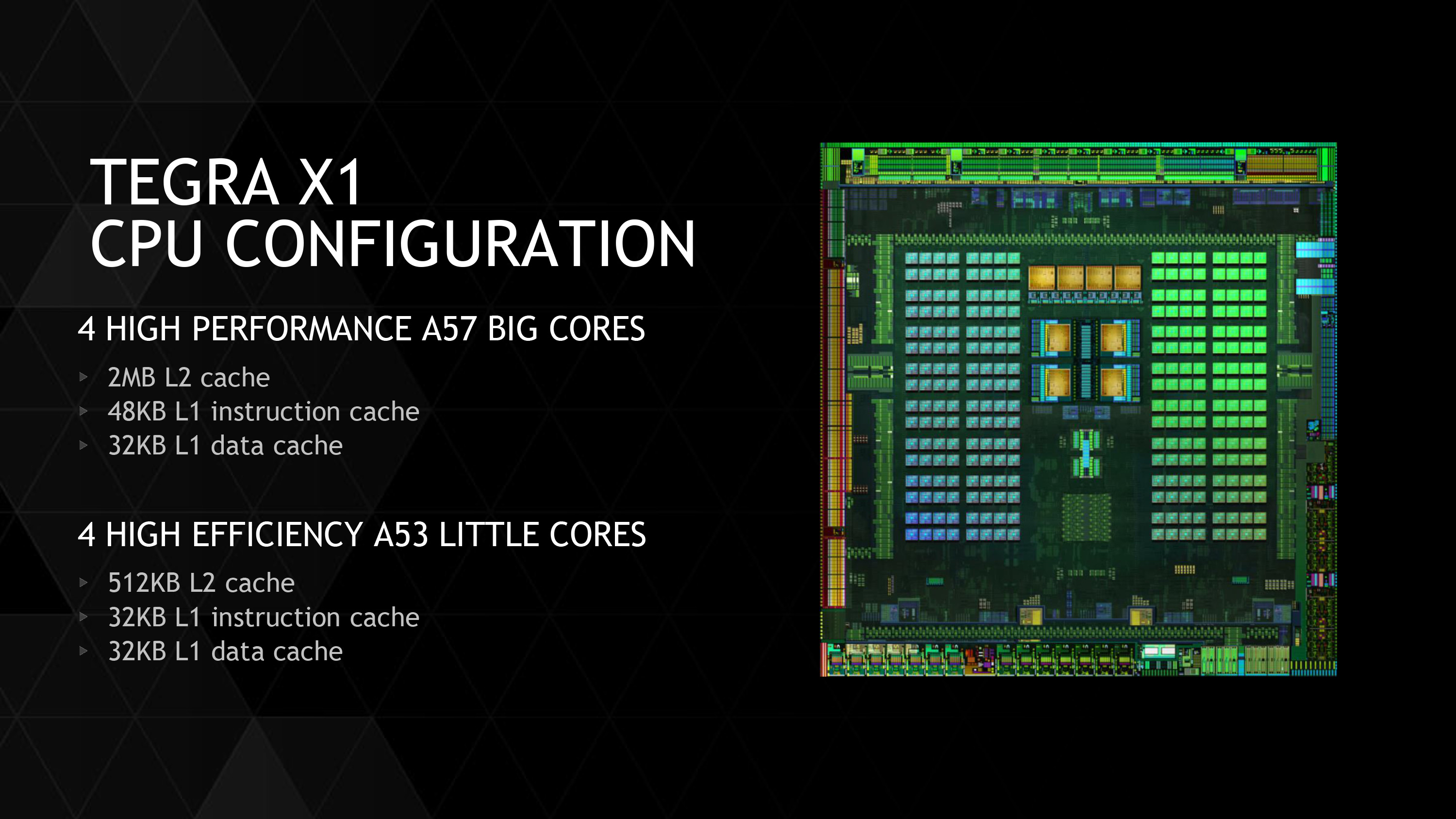
We’ll kick off our look at Erista then with a look at Erista’s CPUs, where one of the bigger surprises in Erista is the CPU configuration. While Tegra K1 had a version with NVIDIA’s custom Denver core for the CPU, NVIDIA has elected to use ARM’s Cortex A57 and A53 in the Tegra X1. The A57 CPU cluster has 2MB of L2 cache shared across the four cores, with 48KB/32KB L1s (I$+D$) per core. The A53 cluster has 512KB of L2 cache shared by all four cores and 32KB/32KB L1s (I$+D$) per core. NVIDIA representatives stated that this was done for time to market reasons.
However, rather than a somewhat standard big.LITTLE configuration as one might expect, NVIDIA continues to use their own unique system. This includes a custom interconnect rather than ARM’s CCI-400, and cluster migration rather than global task scheduling which exposes all eight cores to userspace applications. It’s important to note that NVIDIA’s solution is cache coherent, so this system won't suffer from the power/performance penalties that one might expect given experience with previous SoCs that use cluster migration.
Although cluster migration is usually a detriment to power and performance (especially without a cache coherent interconnect), NVIDIA claims that Tegra X1 significantly outperforms Samsung System LSI’s Exynos 5433 in performance per watt with 1.4x more performance at the same amount of power or half the power for the same performance on the CPU. It's likely that this difference comes from optimizing the implemented logic and differences between Samsung and TSMC 20nm processes rather than differences in thread management. NVIDIA continues to use System EDP (Electrical Design Point) management to control throttling and turbo rather than ARM's IPA (Intelligent Power Allocation) drivers, and in general it seems that while the CPU architecture is ARM's reference design it's quite clear that everything else is distinctly NVIDIA in design.
All of this of course raises the question of where’s Denver, and what is to happen to it? The use of the ARM Cortex A57 and A53, as NVIDIA tells it, was based on a time-to-market decision, and that NVIDIA could bring an off-the-shelf Cortex-based SoC to the market sooner than they could another Denver SoC. On the surface there is at least some evidence to agree with this, as NVIDIA would be able to buy a 20nm design from ARM versus spending the time porting Denver over from TSMC’s 28nm process to their 20nm process. At the same time however integrating an ARM CPU core into an SoC is not an easy task – logic LEGO this is not – so it’s hard to say whether this actually saved NVIDIA much time.
In any case, much like the still in the dark Parker design, NVIDIA is holding their cards close to their chest and hinting that Denver will still be in future generation products. If Parker is still part of NVIDIA’s plans – and they are without a doubt working on some kind of 16nm FF Tegra SoC – then we may still see Denver as part of the original Parker plan. Otherwise at this point while there’s no reason not to believe NVIDIA about the fate of future Denver SoCs, it’s anyone’s guess when we might see it again.
Uncore

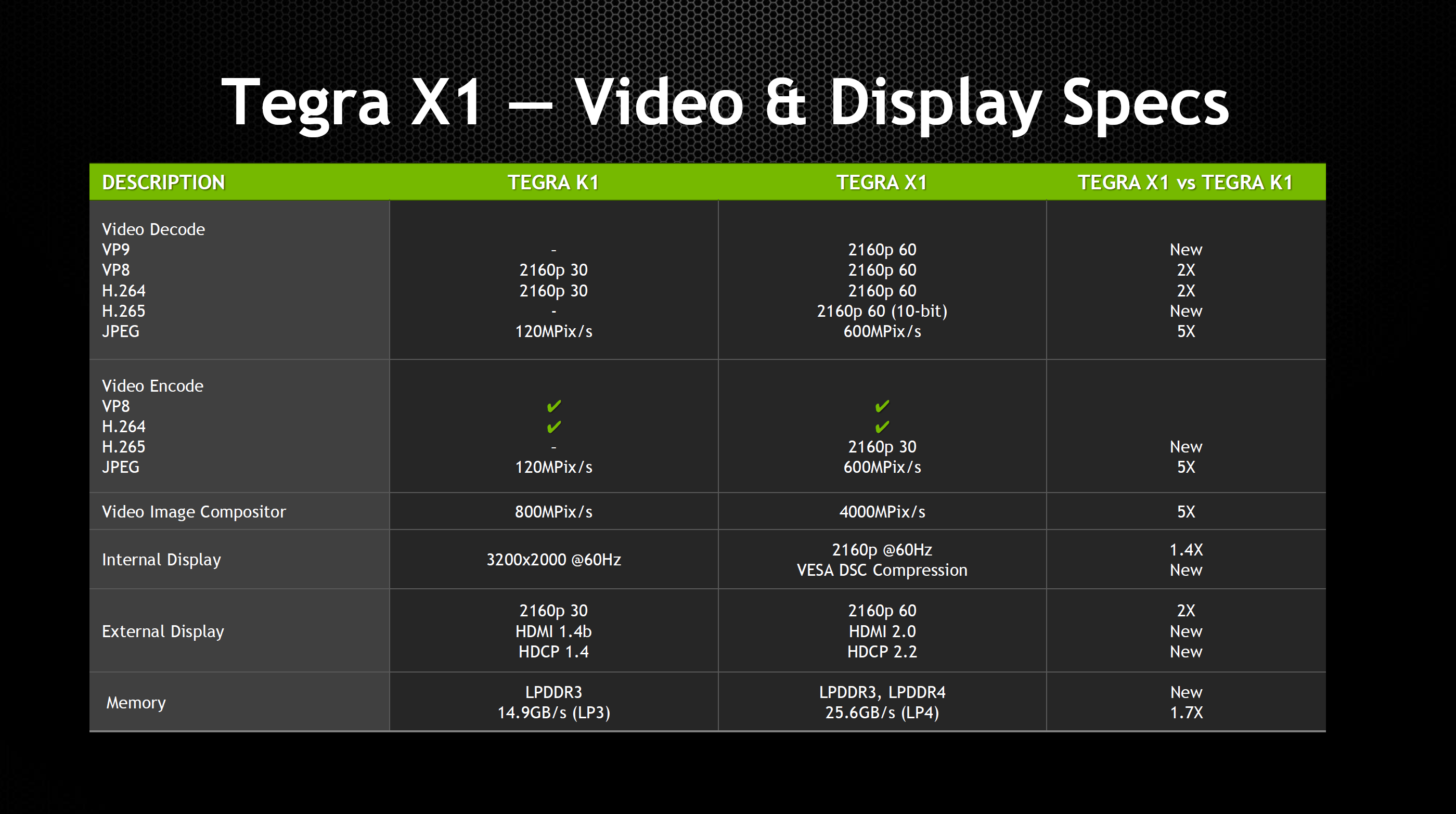
Outside of the CPU and GPU, NVIDIA has also dramatically improved the rest of Tegra X1 in comparison with Tegra K1. We see a move from 64-bit wide LPDDR3 to 64-bit wide LPDDR4 on the memory interface, which improves peak memory bandwidth from 14.9 GB/s to 25.6 GB/s and improves power efficiency by around 40%. In addition, the maximum internal display resolution moves from 3200x2000 at 60 Hz to 3840x2160 at 60 Hz with support for VESA’s display stream compression. For external displays, we see a significant improvement with support for HDMI 2.0 and HDCP 2.2, which means that 4K60 is supported in contrast with the Tegra K1, which only supported 4K30.
The ISP is largely similar to the one we see in the Tegra K1 when it comes to feature set, but JPEG encode and decode rate is now five times as fast, going from 120 MP/s to 600 MP/s. For video encode and decode, we see support for 4K60 H.265 and VP9, with support for 10 bit color on decode on H.265. In addition to support for new codecs in the hardware blocks, we see that H.264 and VP8 now support 4K60, a notable improvement over the 4K30 that was the maximum for Tegra K1. We also see that the storage controller now supports eMMC 5.1 for faster storage performance.


194 Comments
View All Comments
Mayuyu - Monday, January 5, 2015 - link
Apple should start licensing Nvidia GPUs instead of Imagination GPUs for next generation iDevices.twotwotwo - Monday, January 5, 2015 - link
It might be hard (or impossible) for them to do that without breaking compatibility with existing iOS games written around the PowerVR's quirks.Krysto - Monday, January 5, 2015 - link
The OpenGL stuff shouldn't be "impossible". Even the texture compression. I think developers can deal with that. Where Apple really shot itself in the foot is with the launch of the Metal API, though. Now they're stuck with Imagination for at least a few more years until they make it more abstract to work with multiple GPU architectures and not so..."metal". Or they can wait for OpenGL NG to appear, which will probably take just as much time.techconc - Monday, January 5, 2015 - link
How exactly did Apple "shoot itself in the foot" with Metal. They have a solution right now for mobile apps that rivals what is possible on other platforms. All the major game engines have already migrated to Metal. nVidia can show these generic OpenGL benchmarks all they want, but in practice, graphic intensive apps on the A7 and A8 series chips are seeing far greater efficiency and performance improvements.OpenGL NG sounds great in concept, but it takes forever for a consortium like Khronos to develop new standards and just as long for them to eventually be adopted. This is years away from becoming a reality. Yet, Apple gets all of the benefits of that right now. From my perspective, this gives Apple a strong competitive advantage.
akdj - Sunday, January 11, 2015 - link
Well said techconcNot sure if you're in to development, SoC design or just a 'user', Krysto...but BOTH Apple's 'Metal' and language 'Swift' were/are HUGE leaps forward to 'cut' the peanut butter layer on the GPU that is Open GL ES ...so developers have 'direct' access to the 'metal' AKA GPU portion of the SoC. It's an amazing feat in 'software engineering' that helped a huge load on the 'hardware engineering' side of the house....specifically because of this!
I own a Note 4 for my business
I own a 6+ as a personal driver.
The former a quad core, 2.7x Ghz procs and the Adreno 420 and 3GB of 'shared' SoC RAM
The latter, a dual core, 1.5Ghz procs with IT's solution for graphics and 1GB of 'shared' SoC RAM
I love them both, different reasons BUT, Play Asphalt 8 on both. Then tell me 'more muscle, power, RAM, cores or core speed' are the reasons I'm playing a more fluent game on iOS vs android
I'm ambidextrous and enjoy using both. Same in the office or home environment. OS X is primary but I've always had a Windows box since the big 'switch' a decade ago
Point being, software is damn near, and sometimes MORE important than hardware to the end user's experience. No one outside of us dorks, geeks, and pocket protector wearing Homers has a clue what FitFat, latency, core clock speed, or hell....cores for that matter MEAN! They couldn't tell Ya if theyre rocking 1, 2, 3 GB of RAM or NO RAM, lol.
The ultimate end experience is designed and defined by the software and hardware working in synergy WITH a development community willing to step up and develop a million optomized apps for your system. If it's running iOS or Android, you're in luck. Windows, a bit tougher to 'win' and if this SoC does indeed have the power/TDP numbers they're bragging, Apple's never been one to change supply chains
There's a reason Tim is CEO, & that's the biggest. When you're dropping 100,000 products a year, you HAVE to have suppliers that can fulfill your orders and needs
adriaaaaan - Thursday, January 15, 2015 - link
Are you honestly expecting a phone with a weaker GPU pushing 50% more pixels to out perform the other? Of course the iPhone is smoother in games its lower res than the note 4Maleficum - Wednesday, January 21, 2015 - link
Oh yeah, Note4 has to push more pixels than 6+. However, a resolution that high is simply not necessary in first place, and more importantly, over 30% of the pixel data the SoC has to process are nullified by the pentiled AMOLED. What a waste!Maxjonny55 - Saturday, June 20, 2015 - link
Metal has made easier for to access the GPU and the reason apple had done this due the lack of power on there CPUs compared to android device, yes sure GPUs can run apps with extra power but then so what? Open GL has always been doing that! More will know Java and Open GL and easier for development as all hardware vendor apart from apple will optimise hardware for it.I would not want to compare Asphalt 8 between devices as horse power and muscle has nothing to do with it but lazy work on the part of game creators.
Providing access to metal will make a difference to apps no doubt but some apps and not all.. Open GL provides access to GPU not sure why it took apple so long. I have a Nexus 9 and iPad Air 2 and can't see apart from Apple hype what the Air 2 had to offer in performance! Nexus 9 single core out performes the Air 2 and so does the 1 year older GPU..
Wolfpup - Wednesday, September 30, 2015 - link
"lack of power"? Apple's CPUs blow away any other ARM CPUs.Maleficum - Wednesday, January 21, 2015 - link
OpenGL is FAR outdated. It has way too many performance bottlenecks due to the aged design, and doesn't scale very well with modern GPU/CPU architectures.Both MS and Apple recognized this, et voila, Metal and the upcoming DX12 are their answers.
Pity that Android can't keep up with this, stuck with the opensource mess.