NVIDIA Tegra X1 Preview & Architecture Analysis
by Joshua Ho & Ryan Smith on January 5, 2015 1:00 AM EST- Posted in
- SoCs
- Arm
- Project Denver
- Mobile
- 20nm
- GPUs
- Tablets
- NVIDIA
- Cortex A57
- Tegra X1
GPU Performance Benchmarks
As part of today’s announcement of the Tegra X1, NVIDIA also gave us a short opportunity to benchmark the X1 reference platform under controlled circumstances. In this case NVIDIA had several reference platforms plugged in and running, pre-loaded with various benchmark applications. The reference platforms themselves had a simple heatspreader mounted on them, intended to replicate the ~5W heat dissipation capabilities of a tablet.
The purpose of this demonstration was two-fold. First to showcase that X1 was up and running and capable of NVIDIA’s promised features. The second reason was to showcase the strong GPU performance of the platform. Meanwhile NVIDIA also had an iPad Air 2 on hand for power testing, running Apple’s latest and greatest SoC, the A8X. NVIDIA has made it clear that they consider Apple the SoC manufacturer to beat right now, as A8X’s PowerVR GX6850 GPU is the fastest among the currently shipping SoCs.
It goes without saying that the results should be taken with an appropriate grain of salt until we can get Tegra X1 back to our labs. However we have seen all of the testing first-hand and as best as we can tell NVIDIA’s tests were sincere.
| NVIDIA Tegra X1 Controlled Benchmarks | |||||
| Benchmark | A8X (AT) | K1 (AT) | X1 (NV) | ||
| BaseMark X 1.1 Dunes (Offscreen) | 40.2fps | 36.3fps | 56.9fps | ||
| 3DMark 1.2 Unlimited (Graphics Score) | 31781 | 36688 | 58448 | ||
| GFXBench 3.0 Manhattan 1080p (Offscreen) | 32.6fps | 31.7fps | 63.6fps | ||
For benchmarking NVIDIA had BaseMark X 1.1, 3DMark Unlimited 1.2 and GFXBench 3.0 up and running. Our X1 numbers come from the benchmarks we ran as part of NVIDIA’s controlled test, meanwhile the A8X and K1 numbers come from our Mobile Bench.
NVIDIA’s stated goal with X1 is to (roughly) double K1’s GPU performance, and while these controlled benchmarks for the most part don’t make it quite that far, X1 is still a significant improvement over K1. NVIDIA does meet their goal under Manhattan, where performance is almost exactly doubled, meanwhile 3DMark and BaseMark X increased by 59% and 56% respectively.
Finally, for power testing NVIDIA had an X1 reference platform and an iPad Air 2 rigged to measure the power consumption from the devices’ respective GPU power rails. The purpose of this test was to showcase that thanks to X1’s energy optimizations that X1 is capable of delivering the same GPU performance as the A8X GPU while drawing significantly less power; in other words that X1’s GPU is more efficient than A8X’s GX6850. Now to be clear here these are just GPU power measurements and not total platform power measurements, so this won’t account for CPU differences (e.g. A57 versus Enhanced Cyclone) or the power impact of LPDDR4.
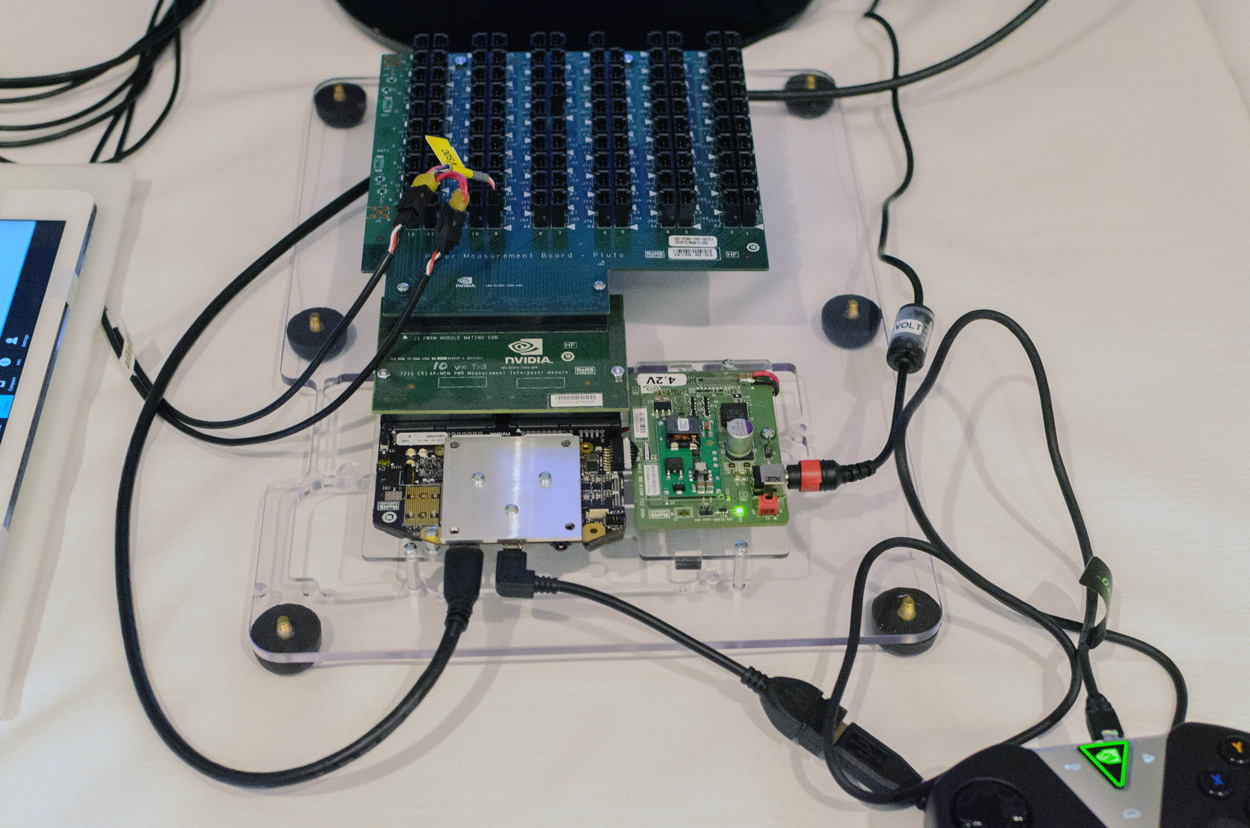
Top: Tegra X1 Reference Platform. Bottom: iPad Air 2
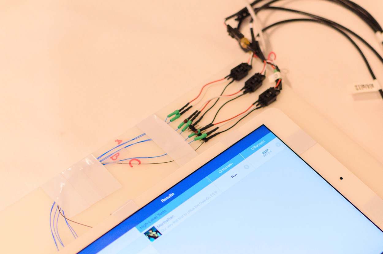
For power testing NVIDIA ran Manhattan 1080p (offscreen) with X1’s GPU underclocked to match the performance of the A8X at roughly 33fps. Pictured below are the average power consumption (in watts) for the X1 and A8X respectively.
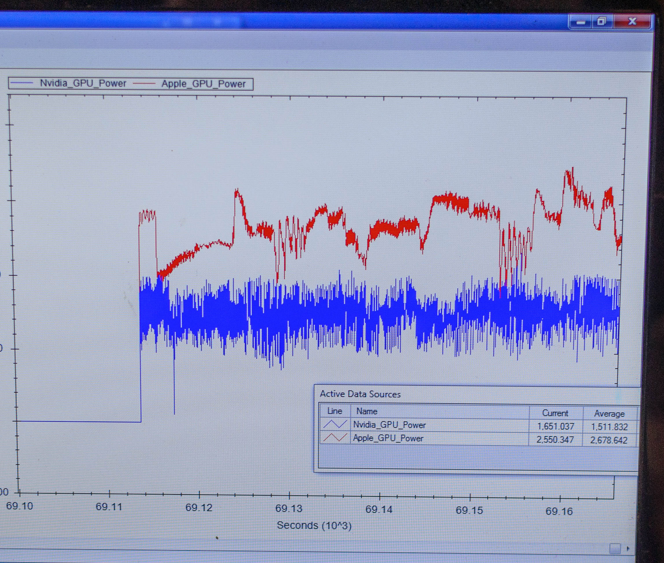

NVIDIA’s tools show the X1’s GPU averages 1.51W over the run of Manhattan. Meanwhile the A8X’s GPU averages 2.67W, over a watt more for otherwise equal performance. This test is especially notable since both SoCs are manufactured on the same TSMC 20nm SoC process, which means that any performance differences between the two devices are solely a function of energy efficiency.
There are a number of other variables we’ll ultimately need to take into account here, including clockspeeds, relative die area of the GPU, and total platform power consumption. But assuming NVIDIA’s numbers hold up in final devices, X1’s GPU is looking very good out of the gate – at least when tuned for power over performance.


194 Comments
View All Comments
Maleficum - Tuesday, January 6, 2015 - link
In fact, Denver IS very special: it's NOT a custom ARM design, but an emulator, a reincarnation of Transmeta's Crusoe/Efficeon.The sad thing is however, that it has TONS of inherent issues, just like the Crusoe/Efficeon.
This time, nVidia did a wise choice by ditching this very questionable design and turned to the traditional native design.
Yojimbo - Tuesday, January 6, 2015 - link
They haven't ditched it. Per at least one top NVIDIA executive, Denver is expected to appear again in future products. Supposedly the reason why Denver is not appearing in the X1 is because it is not ready for the 20nm process shrink, and they want to bring the X1 out faster than Denver would allow. He said Denver is expected to be in 16nm products.chitownbarber - Tuesday, January 6, 2015 - link
Nvidia hired most of the Transmeta engineers, and have implemented at least one similar innovative feature from Transmeta into Denver called Dynamic Code Optimization which optimizes frequently used software routines.Jumangi - Monday, January 5, 2015 - link
Why are you saying "breaking into" an established market? Nvidia was in that market back with the Tegra 2 but their BS claims fell flat when put into real products and device makers abandoned them. They lost their market and now have to win it back again.chizow - Monday, January 5, 2015 - link
Really? What major design wins did the Tegra 2 have at the time? They have always been playing catch up with the likes of Qualcomm, Samsung, even TI back in that time period.At no time has Tegra ever been the market leader in mobile devices, so yeah, so much for that incorrect assertion, clearly they are trying to break into this market and looking at different ways of doing it.
Jumangi - Monday, January 5, 2015 - link
You must have a short memory. Tegra 2 was used in a number of phones because it was the first commercial quad core SoC and companies bought into Nvidia's claims. Then reality came and OEM's abandoned them and they have been trying to turn it around for years now.chizow - Tuesday, January 6, 2015 - link
Which phones? And still nothing even remotely close to the market share captured and retained by the likes of Qualcomm, even TI in that era.As for short memory, again, I believe you are mistaken, Tegra 2 was the first mobile "dual core", perhaps you were thinking of Tegra 3, which is probably still Nvidia's biggest commercial Tegra success but still nothing even remotely close to capturing the market lead as it was going up against the likes of Qualcomm's Snapdragon 400 series.
http://www.nvidia.com/object/tegra-superchip.html
chizow - Monday, January 5, 2015 - link
Also, perhaps the biggest boon of Nvidia's investment in mobile has been their amazing turnaround in terms of power efficiency, which is undoubtedly a result of their investment in mobile GPU designs and the emphasis on lowering TDP.techconc - Monday, January 5, 2015 - link
I would suggest that something like Pixelmator would be a good example of an app that leverages the power of the A8X. Though, I would agree that the A8X is overkill for most apps.DanD85 - Monday, January 5, 2015 - link
Seems to be that the Denver core will take the back seat this year. Judging from the performance of the nexus 9,Denver didn't really set the world on fire as Nvidia previously made it out to be. I think the K1 was relatively a let down last year with limited design win and spotty performance of the Denver architecture. I wonder when will Denver make a come back? 2016?