Chipworks Provides First Apple A7 Die Shot
by Anand Lal Shimpi on September 20, 2013 5:57 PM EST- Posted in
- Smartphones
- Apple
- Mobile
- SoCs
- iPhone 5S
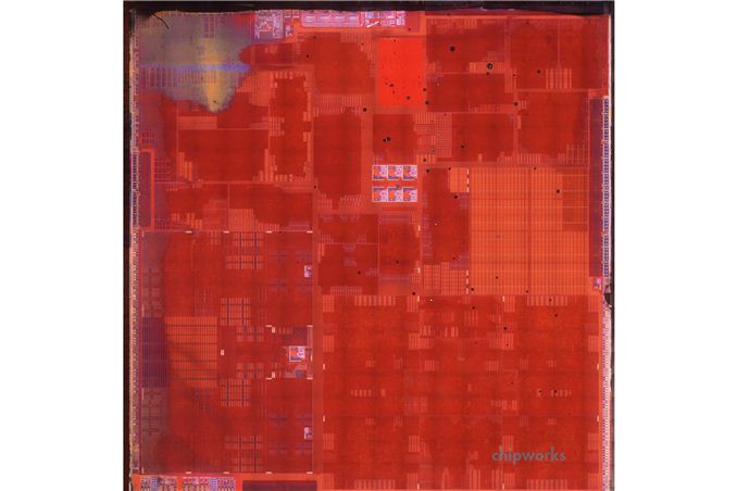
Hot on the heels of their Samsung 28nm confirmation, Chipworks just sent over the first die shot of a delayered Apple A7. An annotated version is following early next week, but I've highlighted two sections of interest:
In yellow we have what appears to be the two Cyclone CPU cores. If those are indeed the two CPU cores, the layout does seem different than what we saw last year with Swift in the A6. Also note that the percentage of die area dedicated to the CPU appears to have grown a small amount (now roughly 17% of the total SoC area).
To the lower right I found four replicated blocks with some shared logic in between (highlighted in light blue). I'm wondering if this area isn't the 4-cluster PowerVR G6430 from IMG. All of this is just a quick educated guess of course.
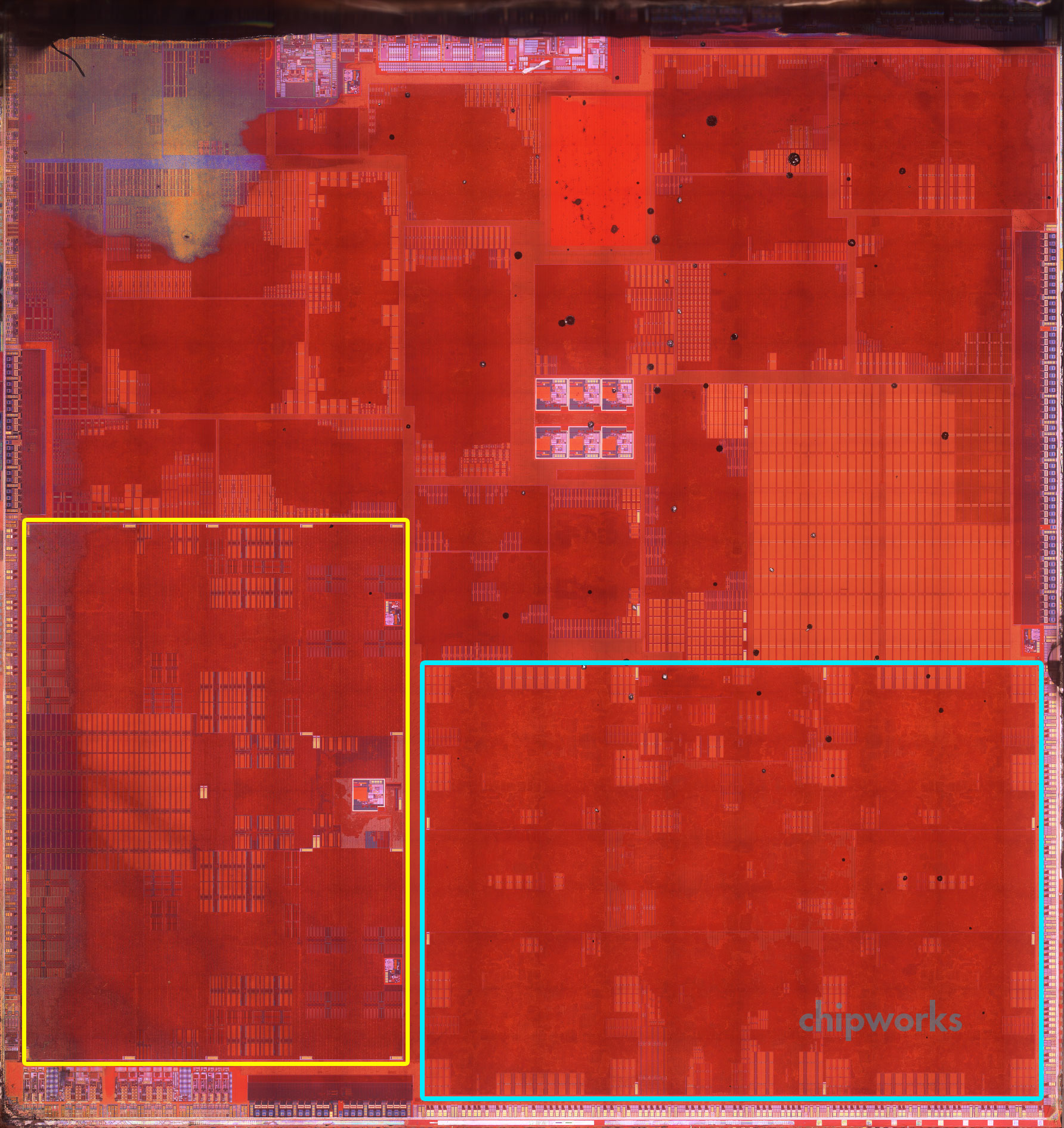 Apple A7, Photo from Chipworks, annotations mine
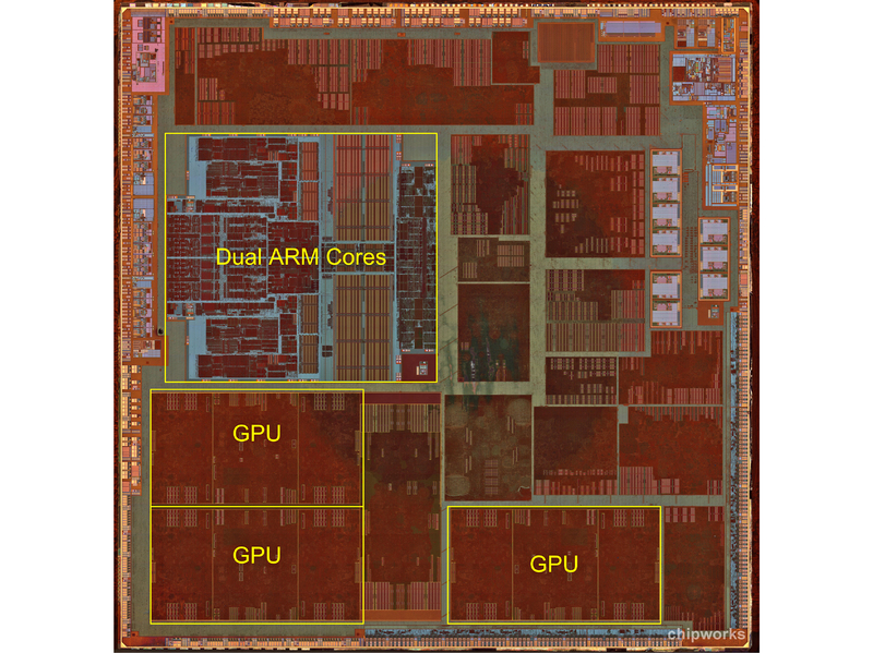 Apple A6, Photo & Annotations from Chipworks
Apple has already confirmed die size (102mm^2) and roughly confirmed transistor count (over 1B) of the A7 so everything else is mostly a known quantity at this point.
| Apple A7 vs A6 SoCs | ||||
| Apple A7 (2013) | Apple A6 (2012) | |||
| Manufacturing Process | Samsung 28nm HKMG | Samsung 32nm HKMG | ||
| Die Size | 102mm2 | 97mm2 | ||
| Transistor Count | "Over 1B" | ? | ||
| CPU | 2 x Apple Cyclone ARMv8 64-bit cores | 2 x Apple Swift ARMv7 32-bit cores | ||
| GPU | IMG PowerVR G6430 | IMG PowerVR SGX 543MP3 | ||
Source: Chipworks


39 Comments
View All Comments
anexanhume - Friday, September 20, 2013 - link
That's a huge block of cache/SRAM above the GPU.tipoo - Friday, September 20, 2013 - link
Looks like it. Built in framebuffer? If you look at the Wii Us GPU, there is something similar on it, a small 1MB SRAM pool, but that's thought to be for Wii backwards compatibility but may have some other interesting performance implications.A5 - Friday, September 20, 2013 - link
Maybe a buffer for the ISP to handle burst mode/slow-motion?tipoo - Friday, September 20, 2013 - link
In a teeny SRAM pool? Not a large chance. That thing is probably ~1MB.SiliconGeezer - Friday, September 20, 2013 - link
The CPU cores look much denser than the A6 cores, together with the new SRAM cache, and the 32-28 shrink it might explain the doubling of transistors 'marketing comments'. This looks like quite a big design change. Congrats to the lab guys at Chipworks, I know these die photos are not easy to make.bartoni - Friday, September 20, 2013 - link
Perhaps it is a 4MB L3 cache. That would explain some of the performance gain.stacey94 - Sunday, September 22, 2013 - link
Isn't cache very power intensive?Samus - Tuesday, September 24, 2013 - link
I don't know, look at Haswell: huge caches, 7-watt CPU's.Rec - Friday, September 20, 2013 - link
Anand in the article you have mentioned Samsung 22nm, is that a typo ? Shouldn't it be 28nm ?Khato - Friday, September 20, 2013 - link
Will certainly be interesting to see what Chipwork's annotated version looks like for the rest of the chip, but I'd be quite surprised if you aren't correct on the CPU and GPU cores.For the fun of it, unless I've made a mathematical error it looks like the 2x Cyclone cores + cache are around 17.76mm^2 while the 2x Swift cores + cache are only 15.82mm^2.