MSI FM2-A85XA-G65 Review: Know Your Platform
by Ian Cutress on December 11, 2012 1:21 AM EST- Posted in
- Motherboards
- MSI
- FM2
- A85X
The A85X chipset and FM2 socket is supposedly here to stay for Trinity plus one more generation. As a result, AMD needs to make sure that the platform is right so that the new processors can slot straight in (whenever that may be). While they may have missed the ship on PCIe 3.0 (despite AMD pioneering it on the GPU side), we do get a tasty array of eight SATA 6 Gbps ports from the chipset with RAID 5 support and a promise that the integrated graphics part of the APU is powerful. In the next installment of our series of FM2/Trinity motherboard reviews, MSI sent us their top line motherboard to test. The FM2-A85XA-G65, while a rather lengthy classification, is a full sized ATX motherboard using the FM2 chipset in an MSI Military Class black and blue theme. At a mid-pack price of $100, MSI gives us the full eight FM2 SATA 6 Gbps ports, 5 fan headers, a full array of video outputs, and special features such as voltage read points and an OC Genie button.
MSI FM2-A85XA-G65 Overview
Unlike the ASUS and ASRock FM2 motherboards we have reviewed so far, MSI takes the stance on A85X a little differently. The major difference is the PCIe slot arrangement, which forgoes the extra PCIe 2.0 x4 from the chipset found on the previous boards. Instead we get more PCIe x1 slots and PCI slots, suitable for any array of add-in card alongside a GPU or two.
The MSI FM2-A85XA-G65 sits in the price bracket at $100, which officially qualifies for the lower end of the FM2 spectrum on Newegg (~$80-$140). On top of the basic functionality that A85X provides (eight SATA 6 Gbps, four USB 3.0), the board has a Realtek ALC892 audio codec, Realtek 8111E audio, up to 2-way CrossfireX compatibility, five fan headers, the full array of video outputs, power/reset buttons, the OC Genie button and voltage read points. These final two distinguish the MSI board from other implementations in the FM2 arena, allowing users to apply a one button overclock (compared to ASRock which requires a button press and ASUS which is a switch), or monitor the voltage points using easy connections.
In terms of design, the heatsinks are relatively large for the power delivery, and in comparison to the ASRock, the board itself looks relatively clean in terms of traces and transistors. This I believe is down to efficiency in design rather than a lack of design. One potentially confusing point in the MSI board however is the placement of the USB 3.0 port in the middle of the board. In this location it lends itself to either a front panel or rear panel implementation, but could easily be blocked by large GPUs with back plates. It is an interesting location, different to what we have seen in the past.
While in the box is nothing special (a standard inclusion for a $100 product), MSI have a strong aesthetic BIOS design and software package that is varied and easy to use. Rather than being rough around the edges, there are obvious areas of improvement – but seemingly less so than some other vendor implementations of the same functionality.
Performance-wise, the MSI seems to drag its heels in our CPU benchmarking suite. As it turns out, the latest BIOS at the time of testing does not seem to apply turbo multipliers correctly. In the BIOS we have a ‘Turbo Frequency’ at 4.0 GHz and ‘Max Turbo Frequency’ at 4.2 GHz (for the A10-5800K) – my own tests could only push the board to 4.0GHz in single thread load. As a result, the OC Genie auto OC options do not push the system as hard, and in single threaded benchmarks the MSI board lags behind - it also looks like the DPC Latency could be affected as well. I have notified MSI about this issue, and no doubt in time it will be resolved. To be fair across all reviews, I use the latest BIOS at the time of putting the board on the test bed, and these are the results I got with the 1.30 BIOS. It should also be noted that the board is a little slower to POST than most (16.75 seconds), and had problems waking from S3 with the keyboard or mouse on default settings.
The MSI has some tough competition and does not really pull itself away from the rest of the pack unless you want easy-to-use physical read points or a nice system of additional software to deal with. When the results are placed side by side with the cheaper $95 ASRock FM2A85X Extreme6, the performance scales are in favor of the ASRock, leaving the MSI as a choice only if you are really gunning for an MSI build.
Visual Inspection
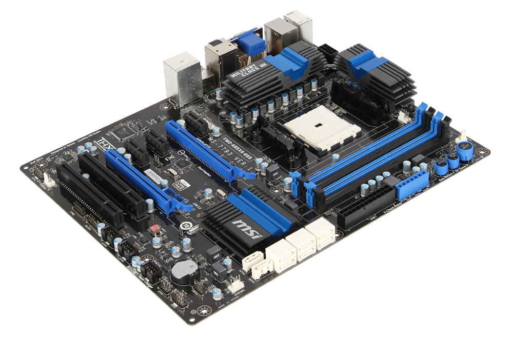
Each of the motherboard manufacturers have a part of their company zeitgeist which is geared towards colors for their products. ASUS use a white to blue scheme for channel boards, red and black for ROG; Gigabyte use a light blue to white on their channel range, green and black for the gaming series then orange and black for the OC boards; ASRock use black and gold for the main range then red/black for Fatal1ty and yellow/black for OC. Given that the MSI logo is blue, blue is bound to feature, and the FM2-A85XA-G65 takes the black and blue very seriously, with everything except the SATA ports using this color scheme – it goes fairly well given the relatively tidy PCB not being covered in silver transistors or traces like some other manufacturers’ products.
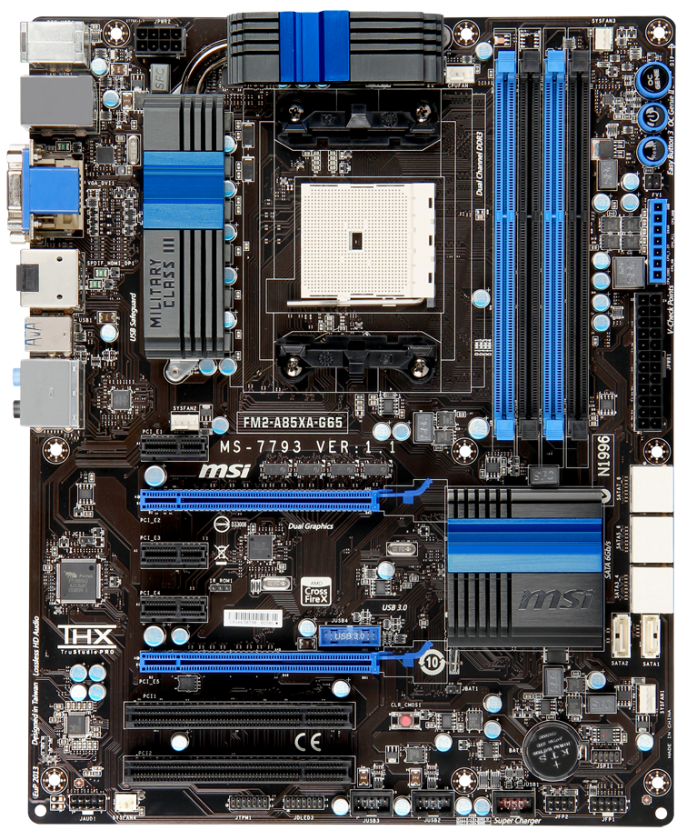
The socket is the typical large AMD socket, and MSI push right up to the AMD recommended distance with their power heatsinks and memory slots. The board has five fan headers, three of which are within easy reach from the socket – one to the right of the VRM heatsink, another to the top right of the board, and a third just above the first PCIe x1 slot. The other two fan headers on board are towards the bottom – one can be found below the SATA ports (and could be blocked by a second GPU), and the other is below the bottom PCI slot.
I would like to point out the ‘cleanliness’ of this MSI board compared to some others. Take a look at the top left compared to the ASRock FM2A85X Extreme6:

Left to Right: MSI, ASRock
The MSI board uses less components and seems highly organized, hence my use of the ‘cleanliness’ word. Having less components means a few things – there is less to go wrong, the motherboard can be produced quicker, and sometimes it overclocks better (from empirical experience). On the flip side, asking other manufacturers about component numbers and placement will usually get the response ‘those components are required’ and could be part of a larger plan for stability based on power delivery or component choice. One could suggest the difference between the two above could be indicative of hardware choices (power delivery phases, IO panel considerations), but it seems more of a feature across the range of certain vendors. By actually speaking with MSI gives us an inkling towards some of the suggestions as to why the difference occurs across vendors – around the board on the right’s components is a white box, used when the machine is placing the components. The MSI board does not use that system, and thus does not need to use the white box and space everything out. An interesting concept put into practice.
Back to the MSI FM2-A85XA-G65, and on the right hand side of the motherboard, we have plenty of functionality to point out. At the top we have an OC Genie button (for a one button overclock), and power/reset buttons. On many other motherboards this combination usually comes with a two-digit debug LED for debugging, but unfortunately not here. Instead we get voltage read-points (which require no soldering) for the extreme enthusiast. Below the 24-pin ATX power connector are our eight SATA 6 Gbps ports in white, with six of them facing out of the motherboard and two facing up. These final two SATA ports (and the fan header below it) are at risk from being covered by a large device in the second PCIe slot.
The chipset heatsink is comparatively slightly smaller than some other motherboards we have seen, but nearby are two interesting design choices. Firstly, the USB 3.0 port is found directly in the middle of the board. This would be to presumably cater for both rear bracket usage and front panel connections – but while it compromises for both it is not ideal for either situation. As an added warning, users of dual GPU setups and cards with backplates may make the USB 3.0 header unusable. You could argue that an FM2/Trinity user would not have dual cards with backplates (or tri-slot cards) as the CPU would not provide enough grunt, making this placement OK, but it is an interesting discussion point. The second design choice to note is a ClearCMOS button to the right of the PCI slots. This small red dot would be obscured by a large GPU, but I am glad it is in a different location to the power/reset buttons and a different shape/size to avoid confusion.

The PCIe slots are separated such that the most extreme of gaming setups on this FM2 board can still use a PCIe x1 or two, and perhaps a PCI slot with dual-length GPUs. I reckon if I was designing a dual PCIe slot board like this, this would be one layout under consideration in a final product – the other one would probably be swapping the last PCIe x1 with the first or last PCI slot, or integrating a PCIe x4 from the chipset.
On the bottom of the board we have our front audio header, a fan header, a TPM header, three USB 2.0 headers (one capable of ‘Super Charging’) and our front panel headers. Perhaps annoyingly the locations for the pins are not put on the PCB for the front panel header, but there is an M-Connector in the box to make this job easier – place the case connections on the M-Connector, then the M-Connector into the board. A similar system is in place on some competitors’ boards.

The rear IO does not offer too much deviation from what a standard FM2/Trinity setup would be expected to have. From left to right we get a combination PS/2 port, four USB 2.0, a Realtek 8111E GbE NIC, VGA output, DVI-D, HDMI, DisplayPort, an optical SPDIF output, two USB 3.0 and audio jacks. It would be interesting to find out what proportion of home users actually use each of the video outputs, and whether there would be any merit in reducing some of them to conversion connectors or rotating them 90 degrees.
Board Features
| MSI FM2-A85XA-G65 | |
| Price | Link |
| Size | ATX |
| CPU Interface | FM2 |
| Chipset | AMD A85X |
| Memory Slots |
Four DDR3 DIMM slots supporting up to 64 GB Dual Channel, 1066-1866MHz |
| Video Outputs |
D-Sub DVI-D HDMI DisplayPort |
| Onboard LAN | Realtek 8111E |
| Onboard Audio | Realtek ALC892 |
| Expansion Slots |
2 x PCIe 2.0 x16 (x16/- or x8/x8) 3 x PCIe 2.0 x1 2 x PCI |
| Onboard SATA/RAID | 8 x SATA 6 Gbps, Supporting RAID 0, 1, 5, 10 |
| USB |
4 x USB 3.0 (Chipset) [2 back panel, 2 onboard] 10 x USB 2.0 (Chipset) [4 back panel, 6 onboard] |
| Onboard |
8 x SATA 6 Gbps 1 x USB 3.0 Header 3 x USB 2.0 Headers 1 x ClearCMOS jumper 5 x Fan Headers 1 x Front Panel Audio Header Power/Reset Buttons OC Genie Button Clear CMOS Button Voltage Checkpoints |
| Power Connectors |
1 x 24-pin ATX Power Connector 1 x 8-pin CPU Power Connector |
| Fan Headers |
1 x CPU (4-pin) 4 x SYS (3 x 4-pin, 1 x 3-pin) |
| IO Panel |
1 x PS/2 Combination Port 4 x USB 2.0 2 x USB 3.0 1 x Realtek GbE NIC D-Sub DVI-D HDMI DisplayPort Optical S/PDIF Output Audio Jacks |
| Warranty Period | 3 Years |
| Product Page | Link |
Our old friend the Realtek NIC/Audio combination is back. This time we get a Realtek ALC892 and 8111E, which as previously mentioned is usually sold as a combination discount to motherboard manufacturers. For a motherboard at $100 or less, it is hard to expect anything less. This MSI board is actually one of very few I have in to test that use all eight SATA 6 Gbps on board – normally one gets partitioned off for eSATA duty. Despite this, I still reckon that the placement of the final two ports on the board could have been better coordinated. More than likely MSI did not find a good enough deal on a 4x2 plastic SATA array for a board, but they had plenty of 3x2 in house – then pricing up a 1x2 was more expensive than 2x1. These sorts of decisions are made day by day in terms of pricing in order to bring costs down, hence why some of the lower tier manufacturers use 8x1 on their products, and the top tier manufacturers make enough motherboards that a 3x2 or 4x2 is cost effective.


11 Comments
View All Comments
Wwhat - Wednesday, December 12, 2012 - link
Perhaps if they can't deliver PCIe3.0 they could make it supply the higher power feed from the PCIe3.0 specs at least? Just am off the cuff marketing idea, feel free to use it0