The Xeon E5-2600: Dual Sandy Bridge for Servers
by Johan De Gelas on March 6, 2012 9:27 AM EST- Posted in
- IT Computing
- Virtualization
- Xeon
- Opteron
- Cloud Computing
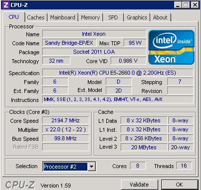
Intel's Sandy Bridge architecture was introduced to desktop users more than a year ago. Server parts however have been much slower to arrive, as it has taken Intel that long to transpose this new engine into a Xeon processor. Although the core architecture is the same, the system architecture is significantly different from the LGA-1155 CPUs, making this CPU quite a challenge, even for Intel. Completing their work late last year, Intel first introduced the resulting design as the six-core high-end Sandy Bridge-E desktop CPU, and since then have been preparing SNB-E for use in Xeon processors. This has taken a few more months but Xeon users' waits are at an end at last, as today Intel is launching their first SNB-E based Xeons .
Compared to its predecessor, the Xeon X5600, the Xeon E5-2600 offers a number of improvements:
A completely improved core, as described here in Anand's article. For example, the µop cache lowers the pressure on the decoding stages and lowers power consumption, killing two birds with one stone. Other core improvements include an improved branch prediction unit and a more efficient Out-of-Order backend with larger buffers.
A vastly improved Turbo 2.0. The CPU can briefly go beyond the TDP limits, and when returning to the TDP limit, the CPU can sustain higher "steady-state" clockspeed. According to Intel, enabling turbo allows the Xeon E5 to perform 14% better in the SAP S&D 2 tier test. This compares well with the Turbo inside the Xeon 5600 which could only boost performance by 4% in the SAP benchmark.
Support for AVX Instructions combined with doubling the load bandwidth should allow the Xeon to double the peak floating point performance compared to the Xeon "Westmere" 5600.

A bi-directional 32 byte ring interconnect that connects the 8 cores, the L3-cache, the QPI agent and the integrated memory controller. The ring replaces the individual wires from each core to the L3-cache. One of the advantages is that the wiring to the L3-cache can be simplified and it is easier to make the bandwidth scale with the number of cores. The disadvantage is that the latency is variable: it depends on how many hops a certain piece of data inside the L3-cache must cross before ends up at the right core.
A faster QPI: revision 1.1, which delivers up to 8 GT/s instead of 6.4 GT/s (Westmere).
Lower latency to PCI-e devices. Intel integrated a PCIe 3.0 I/O subsystem inside the die which sits on the same bi-directional 32 bit ring as the cores. PCIe 3.0 runs at 8 GT/s (PCIe 2.0: 5 GT/s), but the encoding has less overhead. As a result, PCIe 3.0 can deliver up to 1 GB full duplex per second per lane, which is twice as much as PCIe 2.0.
Removing the I/O lowered PCIe latency by 25% on average according to Intel. If you only access the local memory, Intel measured 32% lower read latency.
The access latency to PCIe I/O devices is not only significantly lower, but Intel's Data Direct I/O Technology allows the PCIe NICs to read and write directly to the L3-cache instead of to the main memory. In extremely bandwidth constrained situations (using 4 infiniband controllers or similar), this lowers power consumption and reduces latency by another 18%, which is a boon to HPC users with 10G Ethernet or Infiniband NICs.
The new Xeon also supports faster DDR-3 1600, up to 2 DIMMs per channel can run at 1600 MHz.
Last but certainly not least: 2 additional cores and up to 66% more L3 cache (20 MB instead of 12 MB). Even with 8 cores and a PCIe agent (40 lanes), the Xeon E5 still runs at 2.2 GHz within a 95W TDP power envelope. Pretty impressive when compared with both the Opteron 6200 and Xeon 5600.


81 Comments
View All Comments
BSMonitor - Tuesday, March 6, 2012 - link
My question as well.What is the Intel roadmap for Ivy Bridge in this arena. Would be the same timeframe as IVB-E I would guess.
Wondering if my Intel dividends will pile up enough for me to afford one! Haha
devdeepc - Friday, September 2, 2016 - link
Based on the paper specs, AMD's 6276, 6274 and Intel's 2640 and 2630 are in a neck-and-neck race.fredisdead - Saturday, April 7, 2012 - link
From the 'article' .....'The Opteron might also have a role in the low end, price sensitive HPC market, where it still performs very well. It won't have much of chance in the high end clustered one as Intel has the faster and more power efficient PCIe interface'
Well, if that's the case, why exactly would AMD be scoring so many design wins with Interlagos. Including this one ...
http://www.pcmag.com/article2/0,2817,2394515,00.as...
http://www.eweek.com/c/a/IT-Infrastructure/Cray-Ti...
U think those guys at Cray were going for low performance ? In fact, seems like AMD has being rather cleaning up in the HPC market since the arrival of Interlagos. And the markets have picked up on it, AMD stock is thru the roof since the start of the year. Or just see how many Intel processors occupy the the top 10 supercomputers on the planet. Nuff said ...
iwod - Tuesday, March 6, 2012 - link
And not find a single comment on how and why "making this CPU quite a challenge, even for Intel."In my view It seems Intel is now using Server Market and Atom / SoC for their 32nm capacity when ever they introduce a new node in consumer products.
extide - Tuesday, March 6, 2012 - link
A large part of Intel's long-term strategies include keeping the fabs occupied.Latest gen fabs (currently 22nm) produce bleeding edge cpu's, usually in the consumer space
One gen back (32nm) produces server/workstation/mobile cpus
two gens back (45nm) produces other things like chipsets, and possibly itanium chips
even three gens back (65nm) probably still exists in some places making some chipsets as well.
Their goal is to as much use as possible from their investment into building the fabs themselves.
Kevin G - Tuesday, March 6, 2012 - link
65 nm is still used for Itanium, though the Poulson chip is due sometime this year made on a 32 nm process. If you want to compare die sizes, the 65 nm Tukwila design is 699 mm^2 in size.The main reason why 32 nm Sandybridge-E has been released so close to the release of 22 nm Ivy Bridge chips is that the initial Ivy Bridge chips are consumer centric. Intel performs additional testing on its server centric designs. This is particularly true as Sandybridge-E is not just replacing the dual socket Westmere-EP chips but some of the quad socket Westmere-EX market. RAS demands jump from going from dual to quad socket and that is reflected in additional testing. Implementing PCI-E 3.0 and QPI 1.1 also contributed to the time for additional testing.
Though you are correct that Intel does uses its older process nodes for various chipsets and IO chips. However, as Intel is marching toward SoC designs, the actual utility of keeping these older process nodes in action is decreasing.
meloz - Tuesday, March 6, 2012 - link
>And not find a single comment on how and why "making this CPU quite a challenge, even for Intel."Because it is such a massive die? 416 mm²? Large dies usually have a lower yield, and Intel's 32 nm process is still cutting edge (if only for a few more weeks, heh).
Look at how TSMC, Global Flounderings et al are struggling. An impressive achievement by Intel.
MrSpadge - Tuesday, March 6, 2012 - link
A significant amount of functionality has been added to the SB cores, and Intel can't afford mistakes in such CPUs.BSMonitor - Tuesday, March 6, 2012 - link
More than that though, the SNB-E, Xeon E cores are not duplicates of the SNB desktop cores.Look at Anand's die shot of SNB-E, vs die shot of SNB. The CPU cores, L3 cache, controllers, are arranged completely different. Which makes sense as SNB-E doesn't have to deal with 40% of the die being GPU transistors. So, what we have now with Intel is two completely different dies between Xeon/SNB-E and Core. The individual CPU cores are the same, but the rest of the die is completely different.
SNB-E:
http://www.anandtech.com/show/5091/intel-core-i7-3...
SNB:
http://www.anandtech.com/show/4083/the-sandy-bridg...
cynic783 - Tuesday, March 6, 2012 - link
omg these benches are so biased it's not even funny. everyone knows amd offers clock-for-clock more punch than intel and lower power as well