Micron Breaks Ground on Its $15 Billion EUV DRAM Fab in the U.S.
by Anton Shilov on September 14, 2022 9:00 AM EST- Posted in
- Memory
- Micron
- DRAM
- Semiconductors
- EUV
Micron this week broke ground on its leading-edge memory production facility near Boise, Idaho. The company will invest $15 billion in its new fab as a part of its ambitious plan to invest $40 billion in its U.S.-based manufacturing capacities by the end of this decade as well as spend $150 billion on new fabs by 2030 globally.
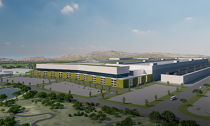
Micron's upcoming leading-edge fab will produce DRAM and will be a rather colossal manufacturing facility. At build-out, when the fab is fully equipped with tools, its cleanroom space will reach 600,000 feet2 (55,700 meters2), which is about two times larger compared to cleanroom space at GlobalFoundries' Fab 8 and which is comparable to cleanroom space at giant fabs operated by Micron's rivals Samsung and SK Hynix is South Korea. Essentially, Micron will operate one of the largest semiconductor production facilities in the U.S.
The new fab will be located adjacent to Micron's R&D center and headquarters near Boise, Idaho, which will bring together scientists, process technology developers, and manufacturing engineers in one location, something that promises to speed up time-to-yield and time-to-market for advanced DRAMs.
"With this facility, Micron will closely couple R&D and manufacturing, providing synergies that will enable us to accelerate the production ramp of advanced memory technology," said Sanjay Mehrotra, president and CEO of Micron.
Micron is currently prepping the site for the new fab and plans to begin construction in early 2023 in a bid to start bringing cleanroom space online gradually starting in 2025. The facility will be equipped with modern deep ultraviolet (DUV) and extreme ultraviolet (EUV) lithography tools and will make memory using one of Micron's advanced EUV-enabled production nodes. The company intends to start fabbing DRAMs at its new facility sometimes in 2025 and then ramp up production to the full capacity in the following years.
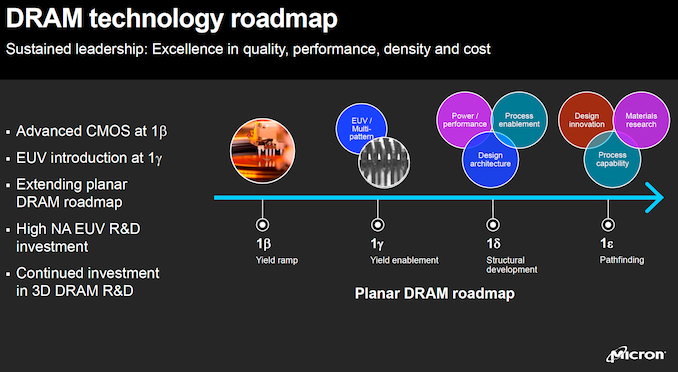
At present it is hard to guess which fabrication process will be adopted at the new fab. Considering the fact that Micron is expected to start DRAM production using its first EUV-enabled manufacturing technology (1γ) sometimes in mid-2023 – early-2024, it is likely that the fab near Boise, Idaho, will adopt the company's second EUV-enabled process (1δ). Yet, this is an educated guess (based on habitual introduction of new DRAM nodes every 18 months or so) at this point.
Micron intends to make 40% of its global DRAM output in America in 2030s, a rebalance that the company has not done in decades. Therefore, in addition to Micron's new fab near Boise, Idaho, the company plans to build a yet another DRAM facility in the U.S. Currently the company is in the final stages of its selection process for another site in America.
Micron will invest $15 billion in the new manufacturing facility near Boise, Idaho. The company also plans to get incentives from the local and state authorities and support from the federal government enabled by the CHIPS and Science act signed into law last month.
"The investment, made possible by the anticipated grants and credits provided by the CHIPS and Science Act, also enhances Micron's supply chain resilience and will establish a new strategic capability for the U.S.," said the head of Micron.
It is noteworthy that Micron is not the only DRAM maker to start building new memory fabs when demand for both 3D NAND and DRAM is down. Last week SK Hynix began to expand its M15 site with its new M15X building as the company is preparing for increased DRAM demand starting in 2025.
Source: Micron


23 Comments
View All Comments
meacupla - Wednesday, September 14, 2022 - link
The most likely reason for Micron building in Idaho, Intel in Arizona, and Samsung in Texas, is because they already have a supply chain running there. Each of those three companies have existing fabs near each of these new $15B fabs.It's very likely that it is cheaper to expand capacity, than to build a whole new supply chain where clean water can be secured, and where there is reliable energy.
Although clean water and reliable energy are important, there is a third, highly time sensitive, and very difficult to manufacture compound. Etching gas for EUV, or extremely pure Hydrogen Fluoride.
Building a plant that can manufacture HF, in the purity needed for EUV, is costly, and takes just as much time as building the chip fab itself.
Ask Samsung how much it cost them to build a HF chemical factory after Japan embargoed HF shipments to Korea in 2019.
Anymoore - Thursday, September 15, 2022 - link
Just a DRAM fab without a NAND fab seems like a mistake, especially since Samsung is expanding in both, as well as foundry.PeachNCream - Thursday, September 15, 2022 - link
Architecture CGI for the facility looks really nice! There are even shadows cast by the trees and, a bus, and some nice little cars in the parking lots. It'd be nice to see that come to fruition in the real world as depicted.