TSMC Roadmap Update: N3E in 2024, N2 in 2026, Major Changes Incoming
by Anton Shilov on April 22, 2022 12:30 PM EST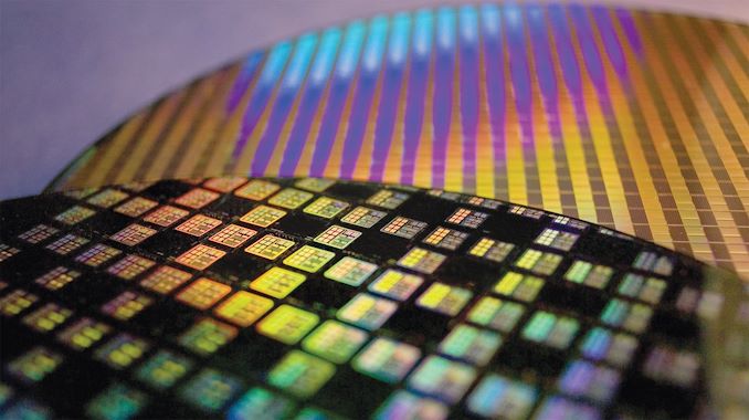
Taiwan Semiconductor Manufacturing Co. has solid plans for the next few years, but the foundry's manufacturing technology design cycles are getting longer. As a result, to address all of its clients' needs, the company will have to keep offering half-nodes, enhanced, and specialized versions of its fabrication processes.
TSMC's success in the last 20 years or so was largely conditioned by the company's ability to offer a new manufacturing technology with PPA (power, performance, area) improvements every year and introduce a brand-new node every 18 – 24 months while maintaining predictably high yields. But as complexity of modern fabrication processes gets to unprecedented levels, it is getting much harder to keep the pace of innovation while also sustaining predictable yields and simple design principles.
With TSMC's N3 node, the gap between N5 (5 nm-class) ramp up and N3 (3 nm-class) ramp up will increase to around 2.5 years, which may pose some challenges to the foundry's key customer, Apple. The good news is that N3's follow up, N3E, seems to be coming in ahead of schedule. Meanwhile, with N2, the cadence is set to stretch to about three years, which largely means a strategic shift in TSMC's strategy of node development.
N3E: An Improved 3nm Node Pulled In (Almost)
TSMC's N3 is set to bring in full node improvements over N5, which includes 10% ~ 15% more performance, 25% ~ 30% power reduction, and an up to 1.7X higher transistor density for logic. To do so, it will use more than 14 extreme ultraviolet (EUV) lithography layers (N5 uses up to 14, and N3 is expected to use even more) and will introduce certain new design rules for deep ultraviolet lithography (DUV) layers.
| Advertised PPA Improvements of New Process Technologies Data announced during conference calls, events, press briefings and press releases |
||||||||
| TSMC | ||||||||
| N7 vs 16FF+ |
N7 vs N10 |
N7P vs N7 |
N7+ vs N7 |
N5 vs N7 |
N5P vs N5 |
N3 vs N5 |
||
| Power | -60% | <-40% | -10% | -15% | -30% | -10% | -25-30% | |
| Performance | +30% | ? | +7% | +10% | +15% | +5% | +10-15% | |
| Logic Area Reduction % (Density) |
70% |
>37% |
- |
~17% |
0.55x -45% (1.8x) |
- |
0.58x -42% (1.7x) |
|
| Volume Manufacturing |
Q2 2019 |
Q2 2020 | 2021 | H2 2022 | ||||
TSMC is set to start ramping up production of chips using its N3 node in the second half of the year and will deliver the first commercial batch to a client (or clients) in early 2023, which is when it will receive the first N3 revenue.
While TSMC's N3 process technology was designed both for high-performance computing (which is a term that TSMC uses to describe applications like CPUs, GPUs, FPGAs, ASICs, etc.) and smartphones in mind, there is evidence that the node has a rather narrow process window, which would make it hard for chip developers to hit desired specifications. This is a problem as it increases time-to-yield and ultimately lowers margins. In an apparent bid to tackle the issue, TSMC has developed N3E version of the technology that widens process window and provides improvements over N5.
"N3E will further extend our N3 family with enhanced performance, power, and yield," said C. C. Wei, chief executive of TSMC.
Originally, TSMC planned to start high-volume manufacturing (HVM) using N3E about a year after N3 (i.e., in Q3 2023), but in the recent months a rumor emerged that TSMC was pulling in HVM of N3E by about a quarter due to better than expected test production runs. During its most recent conference call, TSMC confirmed that N3E's progress was ahead of schedule and that it was considering pulling in mass production using this technology, but did not elaborate about exact plans.
"Our N3E result is quite good," said the head of TSMC. "The progress is ahead of our schedule. And pull-in, yes, we are considering that. So far, I still did not have a very solid data to share with you that how many months we can pull in. But yes, it is in our plan."
Keeping in mind that chip developers have their own schedules for their designs, it is unlikely that all of them will be able to take advantage of earlier N3E ramp since their chips have to pass all the pre-production iterations as well. Nonetheless, better-than-expected N3E progress is a good sign in general, especially considering the fact that TSMC's N3 family will have to serve the industry for quite a long time.
N2: Expect First Chips in 2026
In fact, N3 and its evolutionary iterations will remain TSMC's leading-edge offerings till late 2025 because the company's N2 (2 nm-class) schedule looks quite conservative.
When TSMC first talked about its N2 in August 2020, it did not reveal many details about the technology (by now we know that it adopts gate-all-around [GAA] transistor structure) or its schedule, but indicated that it would build a brand-new fab near Baoshan, Hsinchu County, Taiwan, for this node (some sources call this new facility Fab 20). Taiwanese authorities approved the construction plan in mid-2021 and that plan included breaking ground in early 2022 (earlier this year TSMC's board of directors indeed accepted capital appropriations for a new fab construction), so we believe that the shell is being built as we speak.
Shell construction usually takes a year or a little more, then equipment installation takes over a year as well, so we expect the first phase of Fab 20 to be ready by mid-2024 at the latest. TSMC expects to start risk production using its N2 technology in late 2024 and then initiate HVM towards the end of 2025, which means that the gap between the initial N3 ramp in Q3 2022 and initial N2 ramp in Q4 2025 will be about three years.
"Our progress so far today for the N2 is on track," said Mr. Wei. "All I want to say is, yes, at the end of 2024, [N2] will enter the risk production. 2025, it will be in production, probably close to the second half or the – or the end of 2025. That is our schedule."
Considering how long modern chip production cycles are, it is safe to say that the first N2 chips made by TSMC will arrive in consumer devices no sooner than early 2026.
| TSMC's New Node Introduction in Recent Years | ||||||||
| N7 | N7P | N5 | N5P | N3 | N3E | N2 | ||
| Transistor Type | FinFET | FinFET | FinFET | FinFET | FinFET | FinFET | GAA FET | |
| Risk Production | ? | ? | ? | ? | 2021 | 2022 | Late 2024 | |
| Volume Manufacturing |
Q2 2018 |
Q2 2019 | Q2 2020 |
Q2 2021 | Q3 2022 | Q2/Q3 2023 | Late 2025 | |
But perhaps TSMC's public disclosures about N2 and Fab 20 are too conservative. Analysts from China Renaissance Securities seem to be more optimistic about Fab 20 readiness than TSMC is, which may be an indicator that the foundry could pull-in N2 HVM by a quarter or even two if the fabrication process meets its performance, power, and yield goals.
"We also see more clarity around TSMC's N2 expansion schedule in Fab 20 (Hsinchu)," Sze Ho Ng, an analyst with China Renaissance Securities, wrote in a report for clients. "Tool move-in is expected to start by end-2022, based on company plans, ahead of risk production in late 2024E with Intel (client PC Lunar Lake's graphic 'tiles', while the CPU 'tiles' are fabbed using Intel’s 18A) and Apple being the anchor customers for dedicated capacity support."
Meanwhile, pulling in a node from Q4 2025 to Q3 2025 when alpha customers already set their plans for 2025 may not make a lot of sense, but we will certainly see how things work out with N2.
More N3 Iterations
This year, TSMC's customers that need a leading-edge fabrication process will use the company's N4 technology, which belongs to the N5 family (along with N5, N5P, N4P, and N4X). Essentially, this means that an N5 node will remain TSMC's most advanced offering for three consecutive years.
N3 nodes will also have to serve TSMC's clients for another three years (2023, 2024, 2025), so we are going to see several iterations of this process. So far, TSMC has formally confirmed N3E and N3X (which is another performance-oriented manufacturing technology akin to N4X aimed primarily at CPUs and datacenter ASICs), but I would expect more N3-derived nodes to come to address mainstream SoCs in 2024 ~ 2025.
Keeping in mind that TSMC's FinFET-based N3 will have to stay competitive against GAA-based Samsung's 3GAP and 2GAE/2GAP in 2023 ~ 2025 and Intel's 20A (RibbonFET + PowerVia) in 2024 and 18A (High-NA EUV) in 2025, TSMC's engineers will have to be quite creative with their N3 enhancements.
On the foundry side of things, TSMC will remain ahead of its rivals for quite a while since Intel is not expected to invest significantly in its IFS-dedicated capacity before 2025 (so its 20A and 18A capacities for IFS customers will likely be limited), whereas Samsung Foundry is traditionally behind TSMC when it comes leading-edge capacity and prefers to prioritize its parent company and strategic clients (e.g., Qualcomm). But formal process technology leadership is what TSMC's engineers will have to maintain with N3 and it will be uneasy to do considering how aggressive Intel and Samsung are.
Changes Are Coming
Evidently, TSMC's brand-new process development and ramp up cadence has increased to two-and-a-half years with N3 and will increase to three years with N2, which may be considered as a major slowdown by its key customers. Meanwhile, potential pull-in of N3E is a good sign which shows that the company can make its intra-node advancements fairly quickly. Hence, the main question is how significant will TSMC's intra-node advancements be going forward. This is a question that only time will answer.
In the meantime, it looks like with TSMC's three-year new node development cycle, future intra-node advancements will be significantly more important for the company and its clients than they are today.


21 Comments
View All Comments
name99 - Friday, April 22, 2022 - link
The emotional tone behind this (as opposed to the actual facts) rides an awful lot on the meaning of "full nodes" and how they are labelled. But this is more or less meaningless, as has been stated many many times before!Back in the old days, the equating of "node=sqrt(2) linear shrink" was obvious, but it's been so many years since that was true.
But NOW node seems to mean more something like "substantial change in some aspect of the tech", whether that is adoption of Fins, adoption of EUV, adoption of EUV double-patterning, adoption of GAA, or adoption of back-side power delivery.
In between those large tech changes, we have on-going lithography shrinks of say .9 or so (rather than the .7 of old-school sqrt(2) shrinking) every so often.
This to me does not suggest any sort of doom or even slowdown; it just suggests that things are different. There's more of an emphasis of underlying changes which cause substantial disruption to the fab, less of an emphasis on the on-going small but "routine" improvements that don't require huge fab disruption.
This was probably an inevitable BUSINESS consequence (not TECH consequence). Now that a "real" node change equals a seriously disruptive (and seriously expensive) change in the fab, it becomes not just an engineering issue, it has to be something discussed by finance folks, something negotiated with the huge suppliers, something very very public. Meanwhile the old-style "routine" improvements can be relegated to a less public role because they don't require the same pre-allocation of billions and billions of dollars.
As a side issue, this same analysis points out the ongoing idiocy of Intel's boasting of their i2 and 18A processes. What Intel (or their fanbase don't get) is that the real work of a process now IS that billions and billions of dollars spend, and the outfitting of the next round of fabs. It's NOT the work in the labs, that happens years earlier.
Intel can build the fab shells, cool; but they do not have special access to the ASML and LAM equipment required to populate those fabs. So, come 2024 (or 2022H2 or whenever 18A is now supposed to have moved up to) what Intel will have is a lab that can produce some nice test wafers, not a production line capable of supplying Apple or i5-level demands.
NICOXIS - Friday, April 22, 2022 - link
Intel fought so hard for 10nm, they have to enjoy it at least a decade :Dwhatthe123 - Friday, April 22, 2022 - link
the slowdown is in TSMC's cadence. TSMC has a history of 2~ year cadence on their "new" nodes, which is highly desirable since it gives designers predictable build-refresh-build cycles. it has nothing to do with actual densities and performance targets.at least read the article.
name99 - Sunday, April 24, 2022 - link
At least read the fscking comment!melgross - Monday, April 25, 2022 - link
Oh, it’s definitely a slowdown. All of the small advancements in between the major node reductions are to give clients something to help them sell more chips. I’m not against that, but it indicates that TSMC, and others, are relying on these between node advances to keep things going, somewhat, so that when a full node reduction comes it’s not as spectacular as it once was.Nevertheless, “Moore’s Law” is out the window.
whatthe123 - Monday, April 25, 2022 - link
I did read your comment, and like I said you didn't read the article as it was talking about the update cadence, not some arbitrary performance metric.a 40% power savings a year or two later than usual doesn't exactly help designers when they have to release products every year. that's the slowdown the article is talking about, not the performance figures.
thestryker - Friday, April 22, 2022 - link
It would appear that you have done zero reading regarding Intel's capacity and EUV installations. They've been installing EUV machines in the D1 series of fabs for at least the last couple of years and they're still installing more. Intel is also getting the first High-NA machines from ASML which won't be ready until late 2024/early 2025.The news regarding TSMC is a simple truth that they're slowing down their own cadence of full node releases. This doesn't indicate they're in trouble or that anything is going wrong. They need to give their customers the most concrete information possible and being conservative is very smart. I suspect that TSMC, much like all the leading fabs, is beholden to the rate at which ASML can manufacture EUV/DUV machines.
WaltC - Saturday, April 23, 2022 - link
Nice post. Lots of folks have trouble understanding that Intel is operating in rapid recovery mode, having let their own FABs languish for a decade--waiting on AMD to leapfrog them, again, before attempting to compete, I suppose. Thing is, TSMC has been in heavy development mode along with AMD, as well, which underscores the huge job Intel has ahead of it. There's only so much you can do with marketing, I guess Intel is learning. But when marketing is all you have...well...;) (I know it's not "all" Intel has, but sometimes it is hard to resist, especially when we have anachronisms like Gelsinger announcing he feels relieved "now that he's put AMD in the rear view mirror with Alder Lake"...Who was it who said so aptly..."That would be true only if Intel is moving backwards"...?...;) Intel's time with Apple has definitely rubbed off, imo.Khanan - Sunday, April 24, 2022 - link
Yea, “rear mirror” is hardly the case when your CPU is still 5% slower in total (gaming isn’t relevant for 16 core CPU or at least not their major field), while being auto overclocked and extremely inefficient. Rear mirror isn’t either when you have to give up AVX 512 support and regress in order to do it.That said, Gelsinger is a typical ridicilous Intel guy. His other ridiculous claim was that he will try to win Apple back, which of course is even less likelier to happen since Apple is pretty great in designing their own CPUs and has no interest in giving up control again.
melgross - Monday, April 25, 2022 - link
AMD and Intel can exceed Apple’s performance if they continue to throw more power at it. We see that with their latest designs. Slightly faster in some contexts, but when including GPUs, a good four to five times as much power.I re ember when both AMD and Intel stated that they would t exceed 125 watts. Well, that’s well out the door.