Intel Opens D1X-Mod3 Fab Expansion; Moves Up Intel 18A Manufacturing to H2’2024
by Ryan Smith on April 11, 2022 1:00 PM EST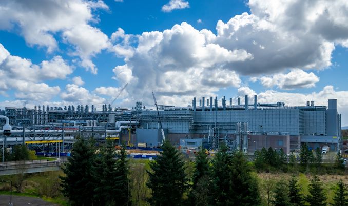
Intel for the last few years has been undergoing a major period of manufacturing expansion for the company. While the more recent announcements of new facilities in Ohio and Germany have understandably taken a lot of the spotlight – especially given their importance to Intel’s Foundry Services plans – Intel has been working even longer on expanding their existing facilities for their own use. The company’s development of next-generation EUV and Gate-All-Around-style transistors (RibbonFET) not only requires creating and refining the underlying technology, but it also just flat out requires more space. A lot of it.
To that end, Intel today is holding a grand opening in Oregon for the Mod3 expansion of D1X, the company’s primary development fab. The expansion, first announced back in 2019, is the third such mod (module) and second expansion for Intel’s main dev fab to be built since D1X’s initial construction in 2010. And in keeping with tradition for Intel fab launches and expansions, the company is making something of an event of it, including bringing Oregon’s governor out to show off their $3 Billion investment.
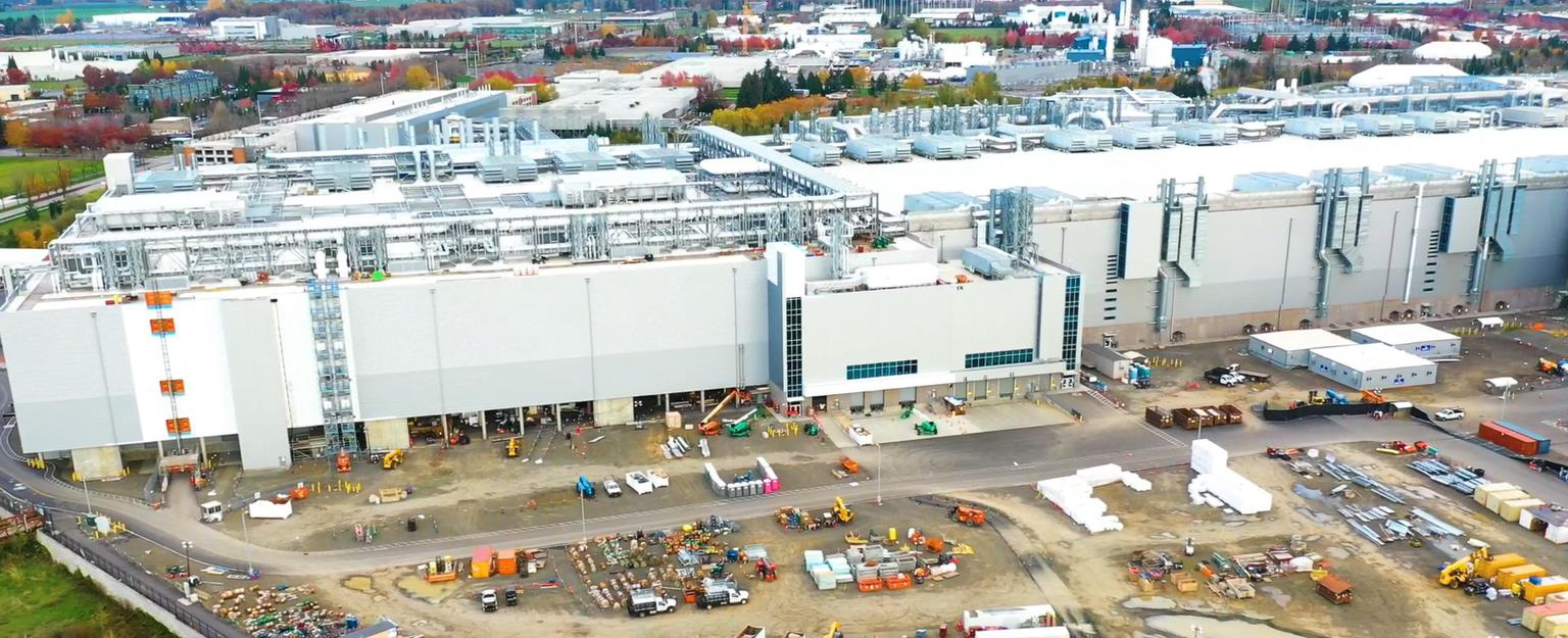
But fanfare aside, the latest mod for the fab is a genuinely important one for Intel: not only does it add a further 270,000 square feet of clean room space to the facility – expanding D1X by about 20% – but it’s the only fab module that’s big enough to support the High Numerical Aperture (High NA) EUV tool that Intel will be using starting with its 18A process. ASML’s forthcoming TWINSCAN EXE:5200 EUV tool is designed to be their most powerful yet, but it’s also quite a bit larger than the NXE 3000 series EUV tools Intel is using for their first generation EUV processes (Intel 4/Intel 3). It’s so big that D1X’s ceiling is too low to fit the machine, never mind the floor supporting its weight.
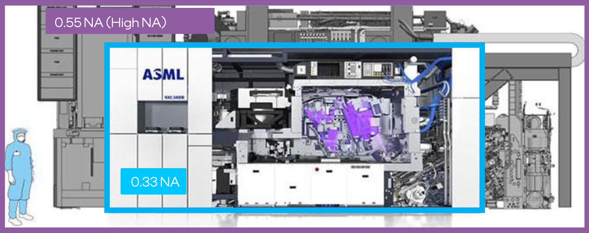
Size Comparison: ASML Normal & High NA EUV Machines
As a result, Mod3 has been built, in no small part, to fit this massive machine. Intel isn’t expecting to take delivery of the machine for a couple more years, but they had to start preparations years in advance just to get to this point.
Meanwhile, although D1X-Mod3 is only being officially declared open today, Intel has already been moving critical tools into Mod3 since last August. Consequently, today’s opening is something of a ceremonial launch for the mod, as parts of it are already setup (if not already in use). Still, even with that head start, according to Intel the company expects to be moving in tools for another year, especially as they bring in the remaining, lower-priority tools.
Coincidentally, our own Dr. Ian Cutress had a chance to see D1X in all of its glory late last year, when he toured the facility. At the time Intel was already in the final stages of finishing the Mod3 expansion, as well as bringing up EUV machines as part of the development of the Intel 4 and Intel 3 process nodes, Intel’s first EUV nodes. So for more information on D1X and what goes on there, be sure to check out that article.
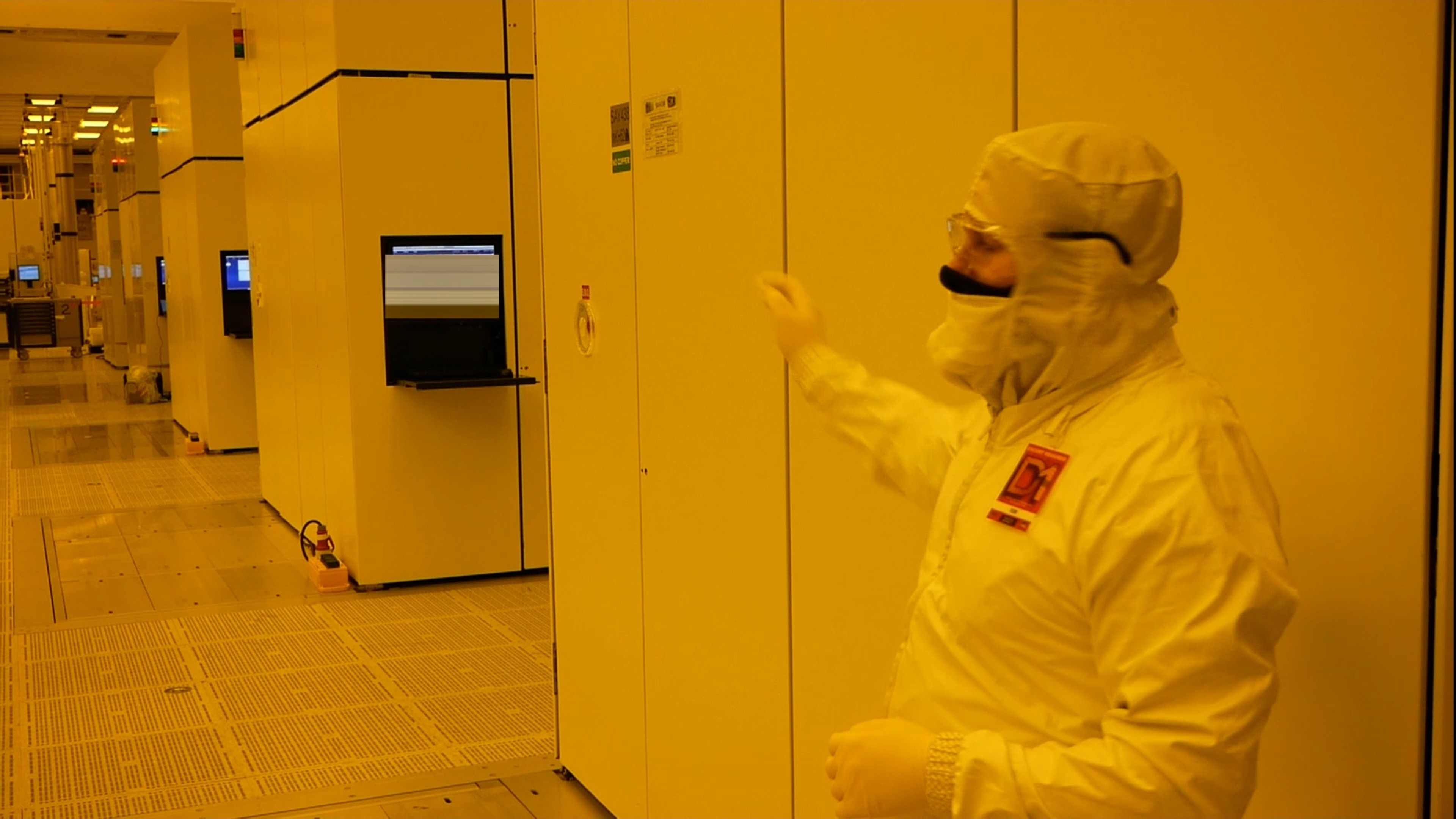
A line of EUV machines at D1X
Finally, along with formally opening the Mod3 expansion, Intel today is also using the opportunity to rename the 450-acre campus that D1X sits on. Intel’s Ronler Acres campus has been the center of Intel’s fab R&D efforts for decades, and along with D1X, also houses Intel’s older D1 development fabs, such as D1B, D1C, and D1D. So, in reflection of all of the important R&D that goes on at the site, Intel is renaming it after co-founder Gordon Moore, one of the instrumental figures behind the development of Intel’s earliest technologies. The newly renamed campus will now go by Gordon Moore Park at Ronler Acres, or Gordon Moore Park for short. And despite the many (many) things that have been named after Moore over the years, from laws and buildings to awards and medals, this is the largest thing named after Moore (yet), as it’s the first time a whole campus has been named after the luminary.

Intel Roadmap Update: Intel 18A Moved Up to H2 2024
Alongside briefing the press about the D1X-Mod3 opening, Intel also used their latest press event to get everyone up to speed on the latest updates on Intel’s development roadmap. Strictly speaking, nothing here is new – all of this was first announced during Intel’s 2022 Investor Meeting back in February. However this is the first time Intel has engaged the technical press, rather than investors, on the current state of its development efforts.
The big news here is that Intel is formally moving up the start date for manufacturing on the Intel 18A node. Intel’s second-generation “angstrom” node was originally expected in 2025; but now the company is bumping that up by half a year, to the second half of 2024.
As a result, Intel’s roadmap now looks like this:
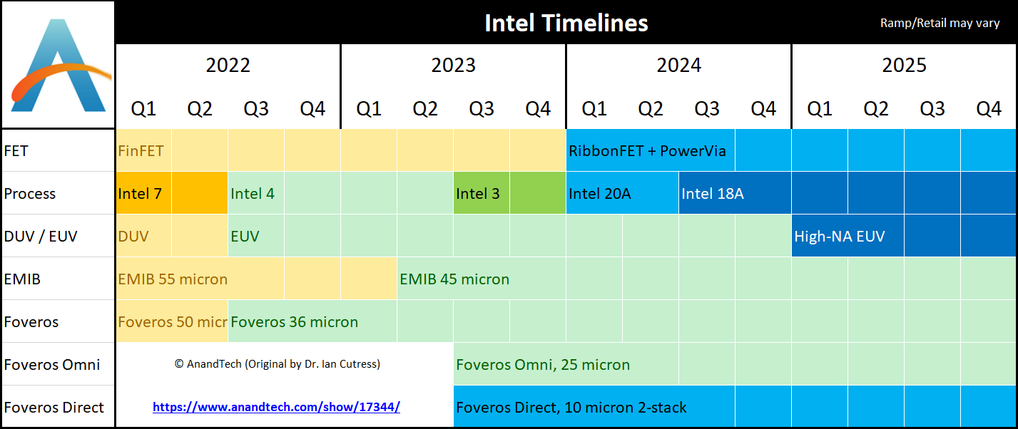
With the company already gearing up for its first EUV process, Intel 4, later this year, Intel’s roadmap starts looking very compressed beginning in the second half of 2023. The second half of that year will see Intel 3 go into production, which is Intel’s enhanced EUV process. Meanwhile, potentially as soon as 6 months after that, Intel 20A goes into production. 20A is Intel’s first “angstrom” node, which incorporates their gate-all-around-style “RibbonFET” FinFets, as well as PowerVias.
But, if all goes according to plan, 20A will seemingly be a relatively short-lived node due to the movement of 18A. Intel’s second-generation angstrom node, which will incorporate an updated ribbon design and other improvements to Intel’s GAA manufacturing technology. Since 18A remains the farthest node out on Intel’s manufacturing roadmaps, the company is remaining relatively mum on everything new that 18A will entail, but it remains the point where Intel plans to re-establish unquestioned leadership of the chip making industry.
According to Intel, 18A development has been moving so well that the company’s R&D operations are now on or ahead of all of their development milestones, giving the company confidence that they can begin manufacturing products based on the process node in late 2024, instead of 2025 as first planned.
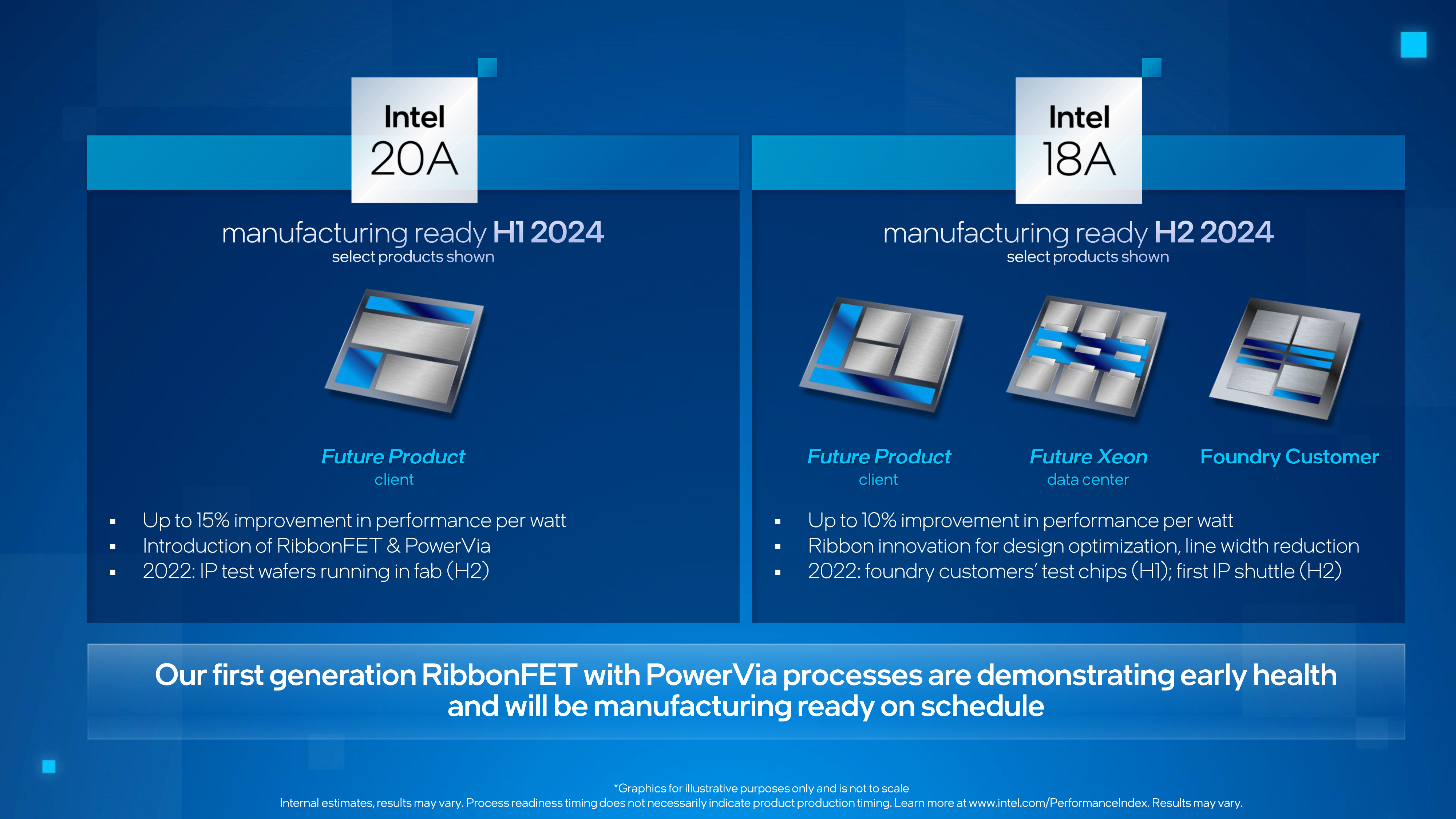
One consequence of bringing in 18A, however, is that it means Intel is now definitely going into initial production of 18A without all of their High NA machines. 18A remains the process node where High NA machines will debut, but as the TWINSCAN EXE 5200 is still not expected to be in place until 2025, that means Intel will now have to use their existing 3000 series machines to kickstart 18A production. Until this latest development, Intel had been presenting High NA machines and 18A as being tied at the hip, so whether that was always the actual case or not, now that is clearly not the case.
What that means for 18A production, in turns, remains to be seen. Since Intel can use their normal (non-HA) machines for 18A, then presumably the biggest advantages of the High NA machines were throughput, allowing Intel to process wafers with little (or not) multi-patterning thanks to High NA’s greater accuracy. Seemingly, the most likely outcome is that Intel will be able to produce 18A in 2024, and maybe even in decent volumes, but that they won’t be able to go into Intel-scale high volume manufacturing until the first High NA machine is available in 2025.
And, as always, it should be noted that Intel’s manufacturing roadmap dates are the earliest dates that a new process node goes into production, not the date that hardware based on the technology hits the shelves. So even if 18A launches in H2’24 as it’s now scheduled, it could very well be a few months into 2025 before the first products are in customer hands, especially if Intel launches in the later part of that window. All of which, given the large size of these launch windows and Intel’s own history, is a likely bet, as Intel has rarely launched new products/technologies early in a release window.
Finally, Intel’s development briefing also included confirmation that Intel is employing a purely internal “test risk reduction” node as part of their development process for their PowerVia technology. The purpose of the test node is to decouple the full risk of 20A by allowing Intel to develop and test PowerVias separately from RibbonFETs. In this case, the test node uses Intel’s well-established FinFET technology on the front-end, while employing a test version of PowerVia on the backend. No such node has been announced for RibbonFETs, but even if one doesn’t exist, not having to debug first-generation PowerVia on 20A alongside the RibbonFETs is still a simplification of the process, as it allows Intel to pursue both elements semi-independently, and learn from both of them in the process.

This is a significant change from how Intel has developed major new manufacturing nodes in the past, and even they are the first to admit as such. Intel’s 10nm problems were caused in large part by bundling too many technology changes together all at once, combined with a very aggressive reduction in feature size. Separating these things into smaller, more frequent manufacturing node updates was one way Intel is mitigating this risk in the future. And now with an internal test node for PowerVia development, they’re aiming to do even more risk mitigation in order to be able to roll out both RibbonFETs and PowerVia together in the first half of 2024 as part of Intel 20A.


89 Comments
View All Comments
mode_13h - Tuesday, April 12, 2022 - link
You're so concerned with competition among CPU makers, but what about ASML? In particular, their exclusive partnership with Intel on high-NA (as in aperture -- not sodium!) is a little troubling.> it's still better than having Intel be burned so badly that
> the investors chose to sell off their foundry business
I still think that would be for the best. I'm glad Intel is starting to treat it more as a separate business, since that will ideally be the eventual outcome.
Calin - Tuesday, April 12, 2022 - link
"18A development has been moving so well that the company’s R&D operations are now on or ahead of all of their development milestones"That does not mean that they will reach risk production as expected, or "real" production numbers as expected. It means that some hard problems were solved, and some other hard problems remain.
As for the additional space needed... improved processes usually take longer (or much longer) per wafer, and (due to the increase in transistor counts) the number of processors per wafer didn't increase much.
Papaspud - Tuesday, April 12, 2022 - link
AMD has shown that when they get on top- they are just as bad as Intel. Look at their latest offerings= r5 5500 4500 and radeon 6500, all total trash products.mode_13h - Wednesday, April 13, 2022 - link
> AMD has shown that when they get on top-So, you think the determining factor was AMD's recent dominance? I say it's the historic chip shortage.
The RX 6500 was designed to be cheap and crypto-unfriendly by cutting die size and memory. The Ryzen 5500 and 4500 are probably just selling off some low-binned APUs at a discount. Right now, I think it's difficult for AMD to provide a better answer to Intel, at the entry level.
Spunjji - Wednesday, April 13, 2022 - link
Some people want AMD to keep offering more than Intel for less money, just so they can buy Intel and talk about how trash AMD's products are.Spunjji - Wednesday, April 13, 2022 - link
"all total trash products"Not really, though. You picked their weakest and cheapest products, all of which serve specific niches and all of which undercut their competition (dramatically in the case of the 6500 XT).
Tom Sunday - Friday, April 22, 2022 - link
Yes indeed in the end we all need someone else to make sure TSMC and likewise offshore friends are kept in check! With Taiwan now being seriously in the crosshairs by China and global superpower territorial expansionism is here to stay, I wonder what that will bring next to our own tech-doorstep? Taiwan as we speak is also not welcomed being a member of the U.N or even considered by many to be a sovereign nation. The good news however is that the USA is now being seen by many as a ‘Safe Harbor’ country. Intel here in Oregon across four campuses in Hillsboro – just ten miles west of Portland just opened its $3-billion expansion with close to 21,000 employees. To date over 65,000 job applications have been received and with people vying for the benefits such as 401K, unrestricted medical and dental, paid vacations, onsite chld care, guaranteed long-term fulltime employment and the top salaries Intel offers. Most certainly and ignoring the technical aspects discussed here for a minute all of this makes me a fan of Intel!wumpus - Saturday, May 7, 2022 - link
Intel will abandon Optane once they can no longer pretend it is dead.If it wasn't fully dead, Micron wouldn't have simply thrown their share of it away. This is rather sad as had it worked, it wouldn't have been a stretch to make huge DRAM caches for vast Optane "main storage". But it don't expect it to ever be more than a really expensive alternative to flash marketed only to enterprise customers.
Silver5urfer - Monday, April 11, 2022 - link
Well it was expected that R&D path that Gelsinger took Intel which it needs is showing. Good to see more R&D on the Lithography side. Especially when we have the total domination by TSMC. A balance needs to be there. Note Samsung is also in the race of GAAFET 3nm same as Intel 3 or 20A / TSMC 3 or 2.But unfortunately, all this tech is going to be wasted on the garbage BGA trash more than HEDT or Mainstream Desktop because that's where these investor riddled companies are at. And worse is E-Core BS that Intel created because of their Intel Core uArch being too old, Nehalem. So until 2025 if the Z990 or Z1000 series chipsets, the Intel Core branding will relegate itself to the pathetic ARM copy cat design of growing more E Cores trash. Maybe by 18A+ with NAEUV Intel will redesign their x86 with a successor to Core. Also hopefully no more BS of awful security holes and tons of papers from Technion students, I have a benefit of doubt how Intel Haifa behaves given the history with NSO Group and Pegasus feud with Apple corporation.
Plus their Xeon will give competition to Bergamo after a whole year, by 2023 Bergamo will be out, and 2024 is when Xeon with E Cores only will come. So Intel is decided on this big small path unfortunately so is AMD but AMD so far doesn't incorporate both into one CPU. I hope they do not do that for Zen 4 or any CPU on AM5. My guess is AMD will make 2 SKU classes, absolute top will be high performance Big trad x86 and the 2nd class would be c cut down versions.
Finally what's the use when the PC itself is seeing weird changes such as Windows 11 going more for BGA Touchscreen dumpster rather than poweruser based UX like Windows 7. And by 2025 and up, not sure how GaaS and these pathetic Service models will fare. So all this tech and growth wasted on such is a massive disappointment.
JayNor - Monday, April 11, 2022 - link
Intel will soon have 16 e-cores on the desktop chips ... Raptor Lake... and the rumors are that will increase to 24 e-cores on the chip after Meteor Lake.I see wccftech reporting a 56 core alder lake-x chip. Will that be mostly e-cores?