Apple's M1 Pro, M1 Max SoCs Investigated: New Performance and Efficiency Heights
by Andrei Frumusanu on October 25, 2021 9:00 AM EST- Posted in
- Laptops
- Apple
- MacBook
- Apple M1 Pro
- Apple M1 Max
Last week, Apple had unveiled their new generation MacBook Pro laptop series, a new range of flagship devices that bring with them significant updates to the company’s professional and power-user oriented user-base. The new devices particularly differentiate themselves in that they’re now powered by two new additional entries in Apple’s own silicon line-up, the M1 Pro and the M1 Max. We’ve covered the initial reveal in last week’s overview article of the two new chips, and today we’re getting the first glimpses of the performance we’re expected to see off the new silicon.
The M1 Pro: 10-core CPU, 16-core GPU, 33.7bn Transistors
Starting off with the M1 Pro, the smaller sibling of the two, the design appears to be a new implementation of the first generation M1 chip, but this time designed from the ground up to scale up larger and to more performance. The M1 Pro in our view is the more interesting of the two designs, as it offers mostly everything that power users will deem generationally important in terms of upgrades.
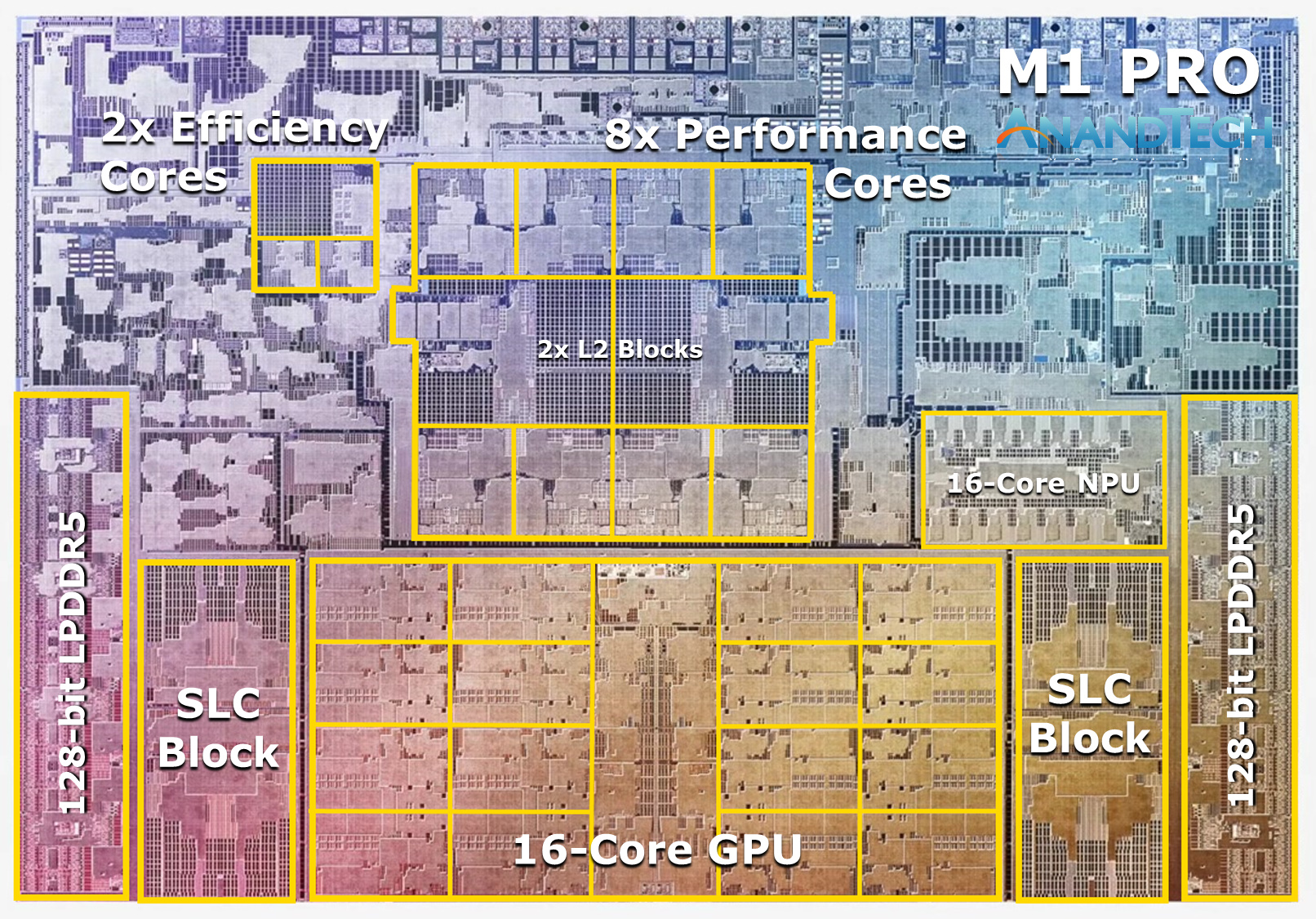
At the heart of the SoC we find a new 10-core CPU setup, in a 8+2 configuration, with there being 8 performance Firestorm cores and 2 efficiency Icestorm cores. We had indicated in our initial coverage that it appears that Apple’s new M1 Pro and Max chips is using a similar, if not the same generation CPU IP as on the M1, rather than updating things to the newer generation cores that are being used in the A15. We seemingly can confirm this, as we’re seeing no apparent changes in the cores compared to what we’ve discovered on the M1 chips.
The CPU cores clock up to 3228MHz peak, however vary in frequency depending on how many cores are active within a cluster, clocking down to 3132 at 2, and 3036 MHz at 3 and 4 cores active. I say “per cluster”, because the 8 performance cores in the M1 Pro and M1 Max are indeed consisting of two 4-core clusters, both with their own 12MB L2 caches, and each being able to clock their CPUs independently from each other, so it’s actually possible to have four active cores in one cluster at 3036MHz and one active core in the other cluster running at 3.23GHz.
The two E-cores in the system clock at up to 2064MHz, and as opposed to the M1, there’s only two of them this time around, however, Apple still gives them their full 4MB of L2 cache, same as on the M1 and A-derivative chips.
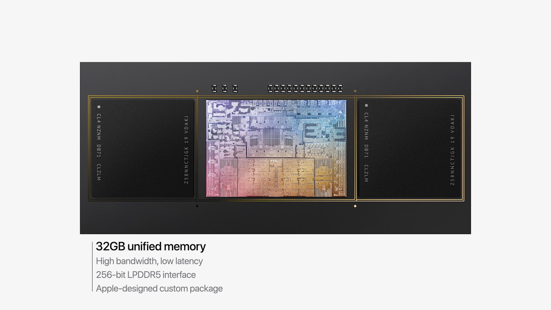
One large feature of both chips is their much-increased memory bandwidth and interfaces – the M1 Pro features 256-bit LPDDR5 memory at 6400MT/s speeds, corresponding to 204GB/s bandwidth. This is significantly higher than the M1 at 68GB/s, and also generally higher than competitor laptop platforms which still rely on 128-bit interfaces.
We’ve been able to identify the “SLC”, or system level cache as we call it, to be falling in at 24MB for the M1 Pro, and 48MB on the M1 Max, a bit smaller than what we initially speculated, but makes sense given the SRAM die area – representing a 50% increase over the per-block SLC on the M1.
The M1 Max: A 32-Core GPU Monstrosity at 57bn Transistors
Above the M1 Pro we have Apple’s second new M1 chip, the M1 Max. The M1 Max is essentially identical to the M1 Pro in terms of architecture and in many of its functional blocks – but what sets the Max apart is that Apple has equipped it with much larger GPU and media encode/decode complexes. Overall, Apple has doubled the number of GPU cores and media blocks, giving the M1 Max virtually twice the GPU and media performance.
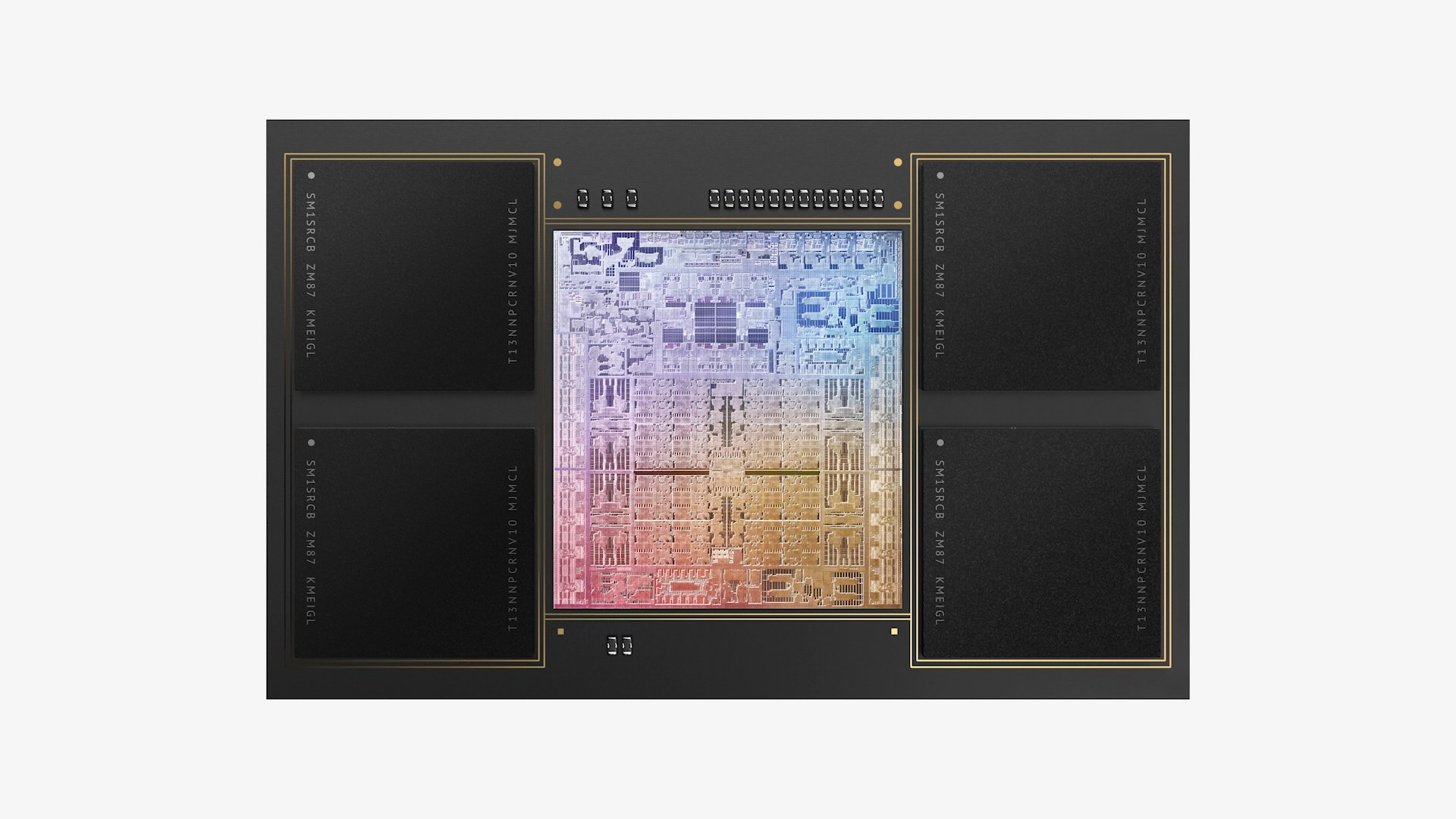
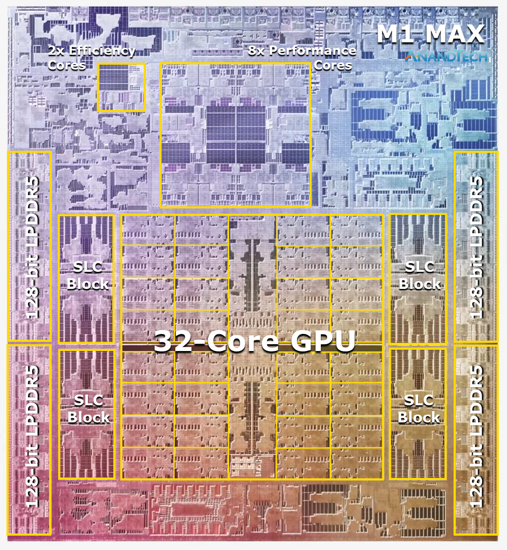
The GPU and memory interfaces of the chip are by far the most differentiated aspects of the chip, instead of a 16-core GPU, Apple doubles things up to a 32-core unit. On the M1 Max which we tested for today, the GPU is running at up to 1296MHz - quite fast for what we consider mobile IP, but still significantly slower than what we’ve seen from the conventional PC and console space where GPUs now can run up to around 2.5GHz.
Apple also doubles up on the memory interfaces, using a whopping 512-bit wide LPDDR5 memory subsystem – unheard of in an SoC and even rare amongst historical discrete GPU designs. This gives the chip a massive 408GB/s of bandwidth – how this bandwidth is accessible to the various IP blocks on the chip is one of the things we’ll be investigating today.
The memory controller caches are at 48MB in this chip, allowing for theoretically amplified memory bandwidth for various SoC blocks as well as reducing off-chip DRAM traffic, thus also reducing power and energy usage of the chip.
Apple’s die shot of the M1 Max was a bit weird initially in that we weren’t sure if it actually represents physical reality – especially on the bottom part of the chip we had noted that there appears to be a doubled up NPU – something Apple doesn’t officially disclose. A doubled up media engine makes sense as that’s part of the features of the chip, however until we can get a third-party die shot to confirm that this is indeed how the chip looks like, we’ll refrain from speculating further in this regard.


493 Comments
View All Comments
OreoCookie - Friday, October 29, 2021 - link
You shouldn't mix the M1 Pro and M1 Max: the article was about the Max. The Pro makes some concessions and it looks like there are some workloads where you can saturate its memory bandwidth … but only barely so. Even then, the M1 Pro would have much, much more memory bandwidth than any laptop CPU available today (and any x86 on the horizon).And I think you should include the L2 cache here, which is larger than the SL cache on the Pro, and still significant in the Max (28 MB vs. 48 MB).
I still think you are nitpicking: memory bandwidth is a strength of the M1 Pro and Max, not a weakness. The extra cache in AMD's Zen 3D will not change the landscape in this respect either.
richardnpaul - Friday, October 29, 2021 - link
The article does describe the differences between the two on the front page and runs comparisons throughout the benchmarks, whilst it's titled to be about the Max I found that it really basically covered both chips, the focus was on what benefits if any the Max brings over the Pro, so I felt it natural to include what I now see is a confusing reference to 24MB because you don't know what's going on in my head 😁From what I could tell the SL cache was not described like a typical L3 cache but I guess you could think of it more like that, so I was thinking of it as almost like an L4 cache (thus my comment about its placement in the die, its next to the memory controllers, and the GPU blocks, and quite far away from the CPU cores themselves so there will be a larger penalty for access vs a typical L3 which would be very close to the CPU core blocks. I've gone back and looked again and it's not as far away as I first though as I'd mistook where the CPU cores were)
Total cache is 72MB (76MB including the efficiency cores' L2, and anything in the GPU), the AMD Desktop M3 chip has 36MB and will be 100MB with the Vcache so certainly in the same ballpark really, as in it's a lot currently (but I'm sure that we'll see the famed 1GB in the next decade). The M1 Max is crazy huge for a laptop which is why I compare it to the desktop Zen3 and also because nothing else is really comparable with 8 cores.
I don't think it's a weakness, it's pretty huge for a 10TF GPU and an 8 core CPU (plus whatever the NPU etc. pull through it). I'm just not a fan of the compromises involved, such as RAM that can't be upgraded; though a 512bit interface would necessitate quite a few PCB layers to achieve with modular RAM.
Oxford Guy - Friday, October 29, 2021 - link
Apple pioneered the disposable closed system with the original Mac.It was so extreme that Jobs used outright bait and switch fraud to sucker the tech press with speech synthesis. The only Mac to be sold at the time of the big unveiling had 128K and was not expandable. Jobs used a 512K prototype without informing the press so he could run speech synthesis — software that also did not come with the Mac (another deception).
Non-expandable RAM isn’t a bug to Apple’s management; it’s a very highly-craved feature.
techconc - Thursday, October 28, 2021 - link
You're exactly right. Here's what Affinity Photo has to say about it..."The #M1Max is the fastest GPU we have ever measured in the @affinitybyserif Photo benchmark. It outperforms the W6900X — a $6000, 300W desktop part — because it has immense compute performance, immense on-chip bandwidth and immediate transfer of data on and off the GPU (UMA)."
richardnpaul - Thursday, October 28, 2021 - link
They're right, which is why you see SMA these days on the newer AMD stuff (Resize BAR) and why Nvidia did the custom interface tech with IBM and are looking to do the same in servers with ARM to leverage these kinds of performance gains. It's also the reason why AMD bought ATI in the first place all those years ago; the whole failed heterogeneous compute (it must be galling for some at AMD that Apple have executed on this promise so well.)techconc - Thursday, October 28, 2021 - link
You clearly don't understand what drives performance. You have a very limited view which looks only at the TFLOPs metric and not at the entire system. Performance comes from the following 3 things: High compute performance (TFLOPS), fast on-chip bandwidth and fast transfer on and off the GPU.As an example, Andy Somerfield, lead for Affinity Photo app had the following to say regarding the M1 Max with their application:
"The #M1Max is the fastest GPU we have ever measured in the @affinitybyserif Photo benchmark. It outperforms the W6900X — a $6000, 300W desktop part — because it has immense compute performance, immense on-chip bandwidth and immediate transfer of data on and off the GPU (UMA)."
This is comparing the M1 Max GPU to a $6000, 300W part and the M1 Max handily outperforms it. In terms of TFLOPS, the 6900XT has more than 2x the power. Yet, the high speed and efficient design of the share memory on the M1 Max allows it to outperform this more expensive part in actual practice. It does so while using just a fraction of the power. That does make the M1 Max pretty special.
richardnpaul - Thursday, October 28, 2021 - link
Yes TFLOPs is a very simple metric and doesn't directly tell you much about performance, but it's a general guide (Nvidia got more out of their hardware compared to AMD for example and have until the 6800 series if you only looked at the TFLOPS figures.) Please, tell me more about what I think and understand /sIt's fastest for their scenario and for their implementation. It may be, and is very likely, that there's some specific bottleneck that they are hitting with the W6900X that isn't a problem with the implementation details of the M1 Pro/Max chips. Their issue seems to be interconnect bandwidth, they're constantly moving data back and forth between the CPU and GPU and with the M1 chips they don't need to do that, saving huge amounts of time because the PCI-E bus adds a lot of latency from what I understand so you really don't want to transfer back and forth over it (and maybe you don't need to, maybe you can do something differently in the software implementation, maybe you can't and it's just a problem that's much more efficiently done on this kind of architecture I don't know and wouldn't be able to comment knowing nothing about the software or problem that it solves. What I don't take at face value is one person/company saying use our software as it's amazing on only this hardware; I mean a la Oracle right?)
When it comes to gaming performance, it seems that the 6900XT or the RTX 3080 seem to put this chip in its place, based on the benchmarks we saw (infact, the mobile 3080 is basically just an RTX 3070 so even more so which could be because of all sorts of issues already highlighted) you could say that the GPU isn't good as a GPU but is great at one task as a highly parallel co-processor for one piece of software that if that's the software you want to use then great for you but if you want to use the GPU for actual GPU tasks it might underwhelm (though in a laptop format and for this little power draw of ~120W max it's not going to do that for a few years which is the point that you're making and I'm not disputing - Apple will obviously launch new replacements which will put this in the shade in time).
Hrunga_Zmuda - Tuesday, October 26, 2021 - link
From the developers of Affinity Photo:"The #M1Max is the fastest GPU we have ever measured in the @affinitybyserif Photo benchmark. It outperforms the W6900X — a $6000, 300W desktop part — because it has immense compute performance, immense on-chip bandwidth and immediate transfer of data on and off the GPU (UMA)."
Ahem, a laptop that tops out at not much more than the top GPU. That is bananas!
buta8 - Wednesday, October 27, 2021 - link
Please tell me how monitor the CPU Bandwidth - Intra-cacheline R&W?buta8 - Wednesday, October 27, 2021 - link
Please tell me how monitor the CPU Bandwidth - Intra-cacheline R&W?