Intel to Launch Next-Gen Sapphire Rapids Xeon with High Bandwidth Memory
by Dr. Ian Cutress on June 28, 2021 12:00 PM EST- Posted in
- CPUs
- Intel
- Xeon
- HBM
- Xeon Scalable
- Sapphire Rapids
- SPR-HBM
As part of today’s International Supercomputing 2021 (ISC) announcements, Intel is showcasing that it will be launching a version of its upcoming Sapphire Rapids (SPR) Xeon Scalable processor with high-bandwidth memory (HBM). This version of SPR-HBM will come later in 2022, after the main launch of Sapphire Rapids, and Intel has stated that it will be part of its general availability offering to all, rather than a vendor-specific implementation.
Hitting a Memory Bandwidth Limit
As core counts have increased in the server processor space, the designers of these processors have to ensure that there is enough data for the cores to enable peak performance. This means developing large fast caches per core so enough data is close by at high speed, there are high bandwidth interconnects inside the processor to shuttle data around, and there is enough main memory bandwidth from data stores located off the processor.
Our Ice Lake Xeon Review system with 32 DDR4-3200 Slots
Here at AnandTech, we have been asking processor vendors about this last point, about main memory, for a while. There is only so much bandwidth that can be achieved by continually adding DDR4 (and soon to be DDR5) memory channels. Current eight-channel DDR4-3200 memory designs, for example, have a theoretical maximum of 204.8 gigabytes per second, which pales in comparison to GPUs which quote 1000 gigabytes per second or more. GPUs are able to achieve higher bandwidths because they use GDDR, soldered onto the board, which allows for tighter tolerances at the expense of a modular design. Very few main processors for servers have ever had main memory be integrated at such a level.
Intel Xeon Phi 'KNL' with 8 MCDRAM Pads in 2015
One of the processors that used to be built with integrated memory was Intel’s Xeon Phi, a product discontinued a couple of years ago. The basis of the Xeon Phi design was lots of vector compute, controlled by up to 72 basic cores, but paired with 8-16 GB of on-board ‘MCDRAM’, connected via 4-8 on-board chiplets in the package. This allowed for 400 gigabytes per second of cache or addressable memory, paired with 384 GB of main memory at 102 gigabytes per second. However, since Xeon Phi was discontinued, no main server processor (at least for x86) announced to the public has had this sort of configuration.
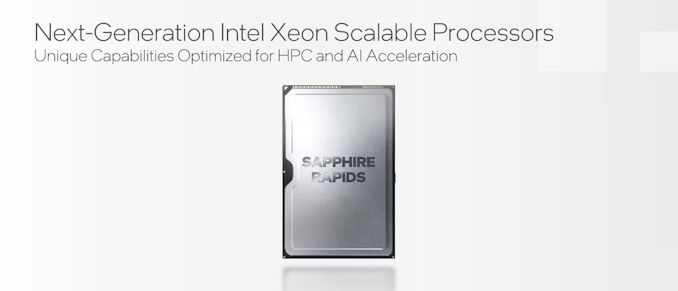
New Sapphire Rapids with High-Bandwidth Memory
Until next year, that is. Intel’s new Sapphire Rapids Xeon Scalable with High-Bandwidth Memory (SPR-HBM) will be coming to market. Rather than hide it away for use with one particular hyperscaler, Intel has stated to AnandTech that they are committed to making HBM-enabled Sapphire Rapids available to all enterprise customers and server vendors as well. These versions will come out after the main Sapphire Rapids launch, and entertain some interesting configurations. We understand that this means SPR-HBM will be available in a socketed configuration.

Intel states that SPR-HBM can be used with standard DDR5, offering an additional tier in memory caching. The HBM can be addressed directly or left as an automatic cache we understand, which would be very similar to how Intel's Xeon Phi processors could access their high bandwidth memory.
Alternatively, SPR-HBM can work without any DDR5 at all. This reduces the physical footprint of the processor, allowing for a denser design in compute-dense servers that do not rely much on memory capacity (these customers were already asking for quad-channel design optimizations anyway).
The amount of memory was not disclosed, nor the bandwidth or the technology. At the very least, we expect the equivalent of up to 8-Hi stacks of HBM2e, up to 16GB each, with 1-4 stacks onboard leading to 64 GB of HBM. At a theoretical top speed of 460 GB/s per stack, this would mean 1840 GB/s of bandwidth, although we can imagine something more akin to 1 TB/s for yield and power which would still give a sizeable uplift. Depending on demand, Intel may fill out different versions of the memory into different processor options.
One of the key elements to consider here is that on-package memory will have an associated power cost within the package. So for every watt that the HBM requires inside the package, that is one less watt for computational performance on the CPU cores. That being said, server processors often do not push the boundaries on peak frequencies, instead opting for a more efficient power/frequency point and scaling the cores. However HBM in this regard is a tradeoff - if HBM were to take 10-20W per stack, four stacks would easily eat into the power budget for the processor (and that power budget has to be managed with additional controllers and power delivery, adding complexity and cost).
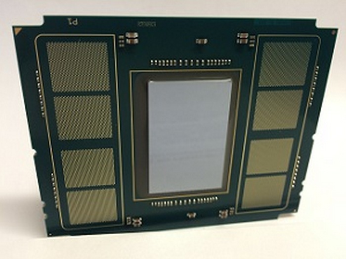
One thing that was confusing about Intel’s presentation, and I asked about this but my question was ignored during the virtual briefing, is that Intel keeps putting out different package images of Sapphire Rapids. In the briefing deck for this announcement, there was already two variants. The one above (which actually looks like an elongated Xe-HP package that someone put a logo on) and this one (which is more square and has different notches):
There have been some unconfirmed leaks online showcasing SPR in a third different package, making it all confusing.
Sapphire Rapids: What We Know
Intel has been teasing Sapphire Rapids for almost two years as the successor to its Ice Lake Xeon Scalable family of processors. Built on 10nm Enhanced SuperFin, SPR will be Intel’s first processors to use DDR5 memory, have PCIe 5 connectivity, and support CXL 1.1 for next-generation connections. Also on memory, Intel has stated that Sapphire Rapids will support Crow Pass, the next generation of Intel Optane memory.
For core technology, Intel (re)confirmed that Sapphire Rapids will be using Golden Cove cores as part of its design. Golden Cove will be central to Intel's Alder Lake consumer processor later this year, however Intel was quick to point out that Sapphire Rapids will offer a ‘server-optimized’ configuration of the core. Intel has done this in the past with both its Skylake Xeon and Ice Lake Xeon processors wherein the server variant often has a different L2/L3 cache structure than the consumer processors, as well as a different interconnect (ring vs mesh, mesh on servers).
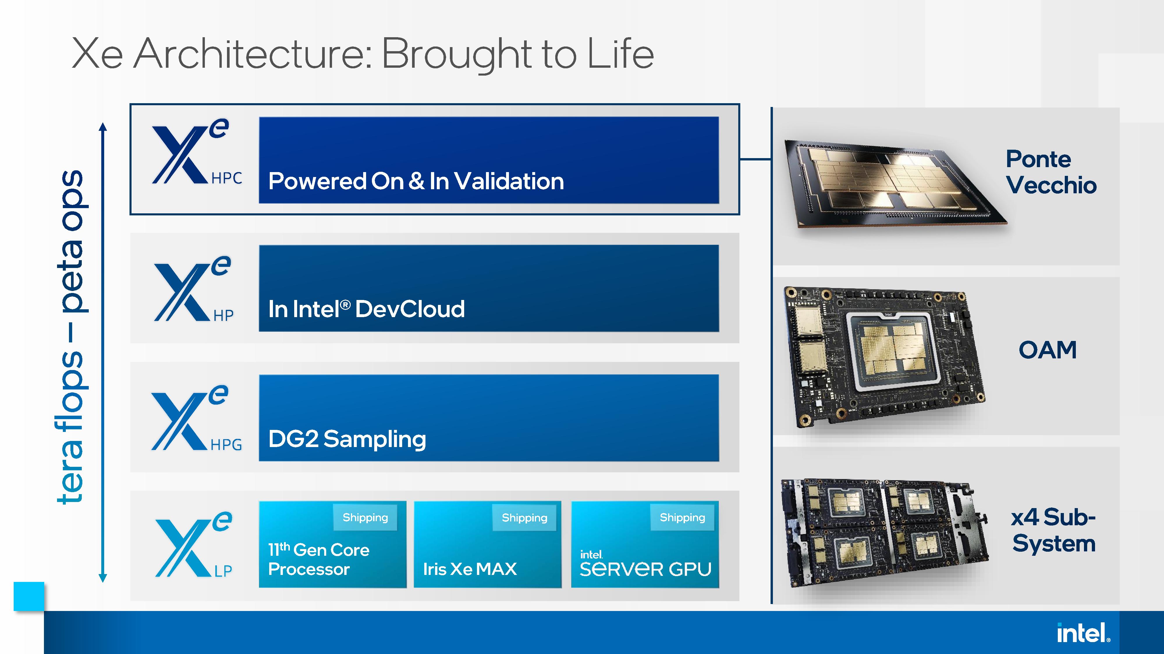
Sapphire Rapids will be the core processor at the heart of the Aurora supercomputer at Argonne National Labs, where two SPR processors will be paired with six Intel Ponte Vecchio accelerators, which will also be new to the market. Today's announcement confirms that Aurora will be using the SPR-HBM version of Sapphire Rapids.
As part of this announcement today, Intel also stated that Ponte Vecchio will be widely available, in OAM and 4x dense form factors:
Sapphire Rapids will also be the first Intel processors to support Advanced Matrix Extensions (AMX), which we understand to help accelerate matrix heavy workflows such as machine learning alongside also having BFloat16 support. This will be paired with updates to Intel’s DL Boost software and OneAPI support. As Intel processors are still very popular for machine learning, especially training, Intel wants to capitalize on any future growth in this market with Sapphire Rapids. SPR will also be updated with Intel’s latest hardware based security.
It is highly anticipated that Sapphire Rapids will also be Intel’s first multi compute-die Xeon where the silicon is designed to be integrated (we’re not counting Cascade Lake-AP Hybrids), and there are unconfirmed leaks to suggest this is the case, however nothing that Intel has yet verified.
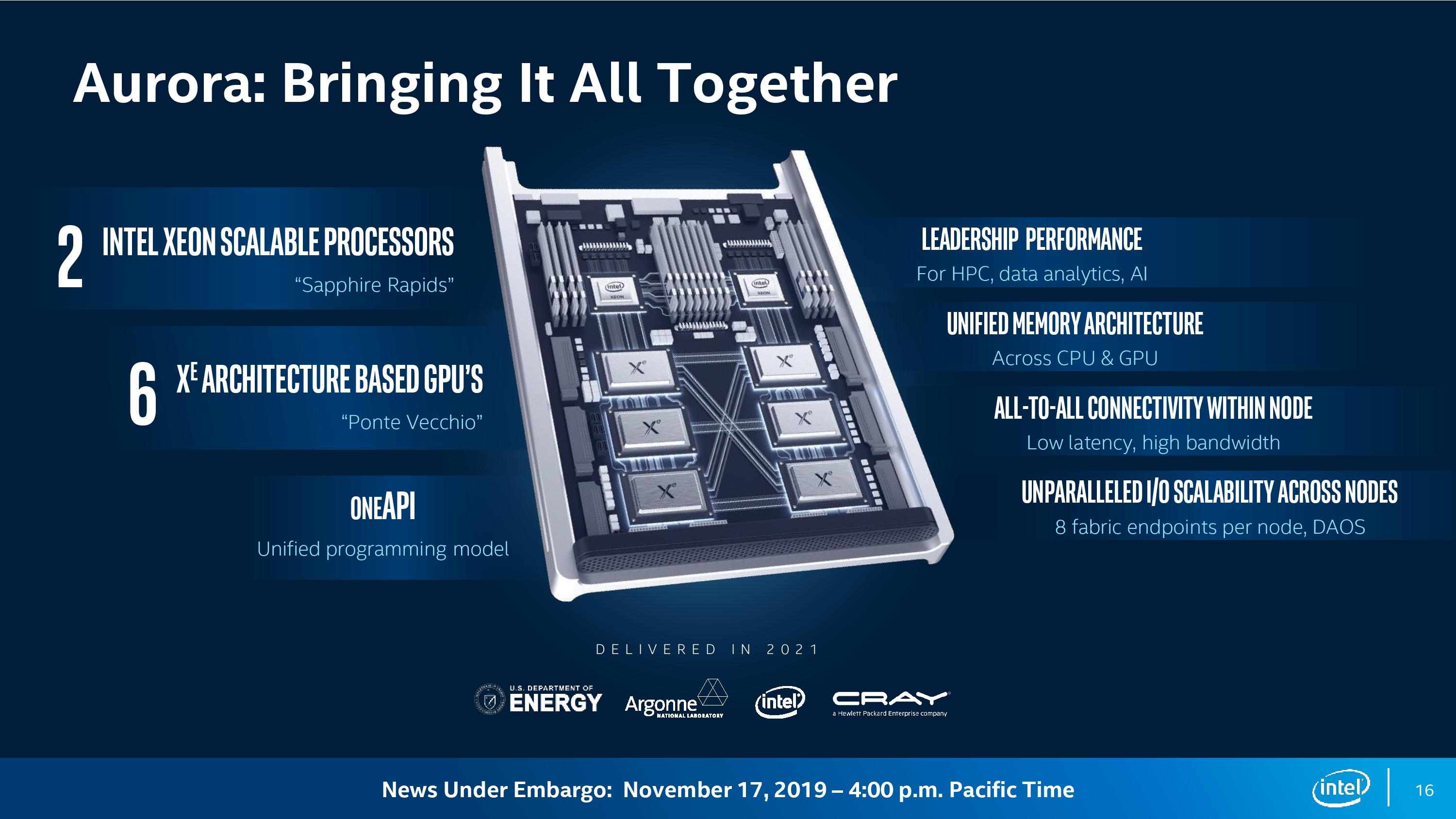
The Aurora supercomputer is expected to be delivered by the end of 2021, and is anticipated to not only be the first official deployment of Sapphire Rapids, but also SPR-HBM. We expect a full launch of the platform sometime in the first half of 2022, with general availability soon after. The exact launch of SPR-HBM beyond HPC workloads is unknown, however given those time frames, Q4 2022 seems fairly reasonable depending on how aggressive Intel wants to attack the launch in light of any competition from other x86 vendors or Arm vendors. Even with SPR-HBM being offered to everyone, Intel may decide to prioritize key HPC customers over general availability.
Related Reading
- SuperComputing 15: Intel’s Knights Landing / Xeon Phi Silicon on Display
- A Few Notes on Intel’s Knights Landing and MCDRAM Modes from SC15
- Intel Announces Knights Mill: A Xeon Phi For Deep Learning
- Intel Begins EOL Plan for Xeon Phi 7200-Series ‘Knights Landing’ Host Processors
- Knights Mill Spotted at Supercomputing
- The Larrabee Chapter Closes: Intel's Final Xeon Phi Processors Now in EOL
- Intel’s 2021 Exascale Vision in Aurora: Two Sapphire Rapids CPUs with Six Ponte Vecchio GPUs
- Intel’s Xeon & Xe Compute Accelerators to Power Aurora Exascale Supercomputer
- Hot Chips 33 (2021) Schedule Announced: Alder Lake, IBM Z, Sapphire Rapids, Ponte Vecchio
- Intel’s Full Enterprise Portfolio: An Interview with VP of Xeon, Lisa Spelman
- What Products Use Intel 10nm? SuperFin and 10++ Demystified
- Intel 3rd Gen Xeon Scalable (Ice Lake SP) Review: Generationally Big, Competitively Small


149 Comments
View All Comments
mode_13h - Wednesday, June 30, 2021 - link
You mean like CAPI or CXL memory devices? Or are you talking about something else?Wereweeb - Monday, July 5, 2021 - link
Not memory through PCIe, Jesus, I mean something like IBM's OMI.Geef - Tuesday, June 29, 2021 - link
Quote: The Aurora supercomputer is expected to be delivered by the end of 2021, and is anticipated to not only be the first official deployment of Sapphire Rapids, but also SPR-HBM. We expect a full launch of the platform sometime in the first half of 2022, with general availability soon after.---
Hey guys you forgot to account for the time delay Intel has EVERY SINGLE TIME a chip comes out. Move each year up by 1 and we should be good. If your feeling nice move it up by two quarters instead.
Atari2600 - Tuesday, June 29, 2021 - link
So what makes this not a day late and dollar short when compared to AMD's stacked L3??Looks slower, more energy intensive and of similar size.... am I missing something?
Ian Cutress - Wednesday, June 30, 2021 - link
This HBM will be alongside the CPU, not on top of it.HBM is higher capacity than AMD's stacked SRAM
Atari2600 - Wednesday, June 30, 2021 - link
Ah, EPYC may run up to around 1GB of L3 - whereas this is an order of magnitude more.Dunno where I got myself mixed up thinking the stacked L3 would also be multiples of GB. Maybe confused in how many layers they were using or something.
I suppose going off at a tangent - is this seen as L4 cache by CPU memory controller? Or is it seen as system RAM?
mode_13h - Thursday, July 1, 2021 - link
> is this seen as L4 cache by CPU memory controller? Or is it seen as system RAM?Didn't they say it supported both modes? Supposedly, that's how Xeon Phi implemented MCDRAM.
Atari2600 - Wednesday, June 30, 2021 - link
Oh - and did you get my email about using the openFOAM benchmark for your server/workstation comparisons? Be a very useful addition that would stress both memory controller and FPU.mode_13h - Wednesday, June 30, 2021 - link
HBM2 provides slower access than AMD's stacked L3 innovation, but scales to about 100x larger data sizes. For instance, if your dataset is like 40 GB, and you're accessing it pretty randomly, Intel's HBM2 is probably going help a lot more than AMD's larger L3 cache.The way I look at them is complementary. For some purposes, the best option would certainly be to have both!
mode_13h - Wednesday, June 30, 2021 - link
To understand why this scales better, remember that HBM is DRAM, which is denser & more power-efficient than SRAM. Also, HBM can currently be stacked up to 12-high, where as AMD's approach only appears to work for adding one extra layer to the compute die.