TSMC Manufacturing Update: N6 to Match N7 Output by EOY, N5 Ramping Faster, Better Yields Than N7
by Andrei Frumusanu on June 1, 2021 5:00 PM EST- Posted in
- Semiconductors
- TSMC
- N6
- N7
- N5
At this year’s TSMC Technology Symposium, the company took the opportunity to update its customers and industry onlookers on the semiconductor manufacturer’s latest developments in regards to its newest technologies and manufacturing roadmaps. As part of a regular presentation, the foundry updated us on its status on it’s current leading-edge manufacturing technologies, the N7, N5 and their respective derivatives such as N6 and N5.
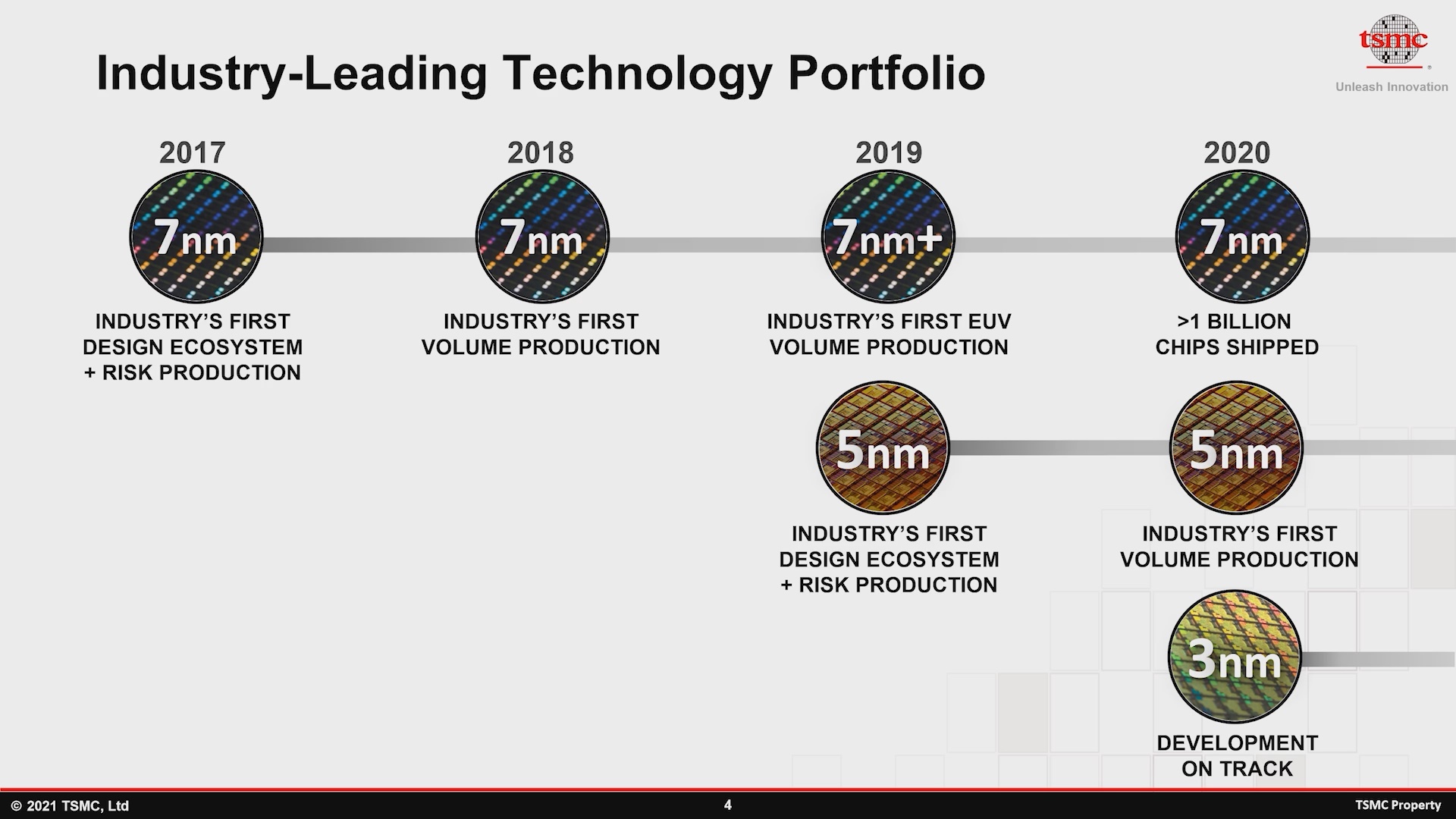
TSMC segregates their leading-edge manufacturing nodes into three product “families”: 7nm, 5nm and the upcoming 3nm manufacturing node. As many will have noted through a wide range of products over the last couple of years, TSMC’s 7nm node introduction and mass manufacturing starting in 2018 was a true tour de force for the foundry, carving out a significant leadership in the industry that the nearest competitors have been struggling to keep up with to this day.
To date, TSMC has shipped over 1 billion 7nm chips, and the 7nm family is regarded as being extremely mature, with the foundry now focusing on ramping up 5nm products and upcoming 3nm advanced nodes.
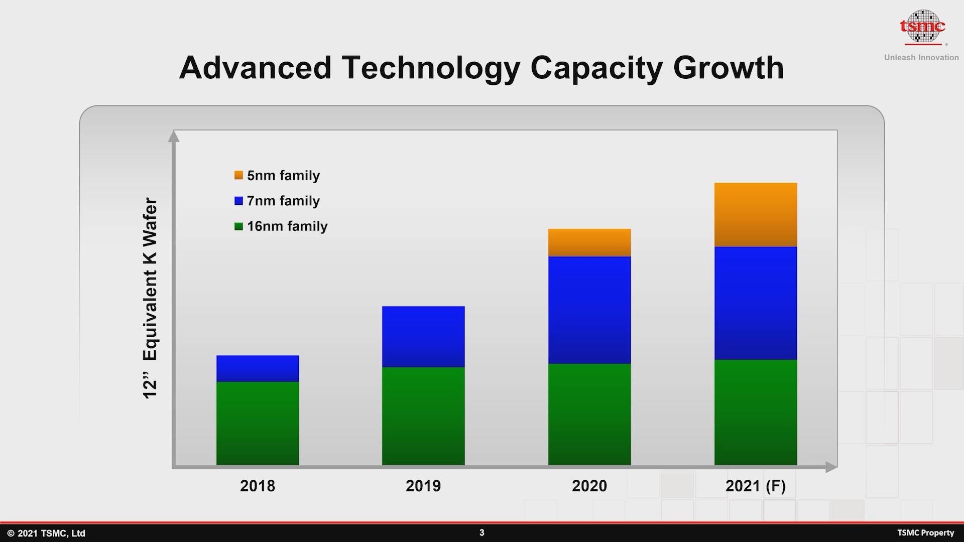
In terms of 7nm family capacity, starting in 2021 the yearly installed capacity is truly starting to slow down significantly as many customers migrate over to the more advanced process nodes.

Forecast capacity projections for 2021 only include a 14% increase in 7nm family capacity – starting a slow pace that’s likely to mimic the foundry’s capacity progression for the older 16nm process family.

Although many customers are shifting towards 5nm and below, the 7nm family will remain very significant for revenue, manufacturing capacity, and customer value. The N6 node is an evolutionary design of the previous N7 node variations and simplifies the manufacturing steps by introducing light usage of EUV layers.
What’s been extremely surprising to see is the rate of adoption of N6 and how it is replacing N7 manufacturing volume: In 4Q20 the N6 node only accounted for 15% of the whole 7nm family manufacturing capacity, while this is expected to reach 48-50% one year later by 4Q21. This means that as we’re speaking, we’re seeing a lot of new ramps of brand-new high-volume N6 products, which is quite interesting. The usual suspects would be vendors such as MediaTek and their newest Dimensity SoCs, but we’ve also seen Qualcomm reveal 6nm mid-range SoC designs such as the Snapdragon 778G. We’ve yet to hear about N6 production from PC or HPC vendors, but given the large volume ramp, one could very well imagine that there must be some new products in those industry sectors as well.
5nm Capacity to Quadruple by 2023 over 2020
TSMC’s 5nm process node has been in mass production since 2020, and notably powers hundreds of millions of new SoCs powering Apple’s A14 chips in the iPhone 12 series as well as the new M1 Mac chip. Although HiSilicon was a lead customer of TSMC at 5nm, TSMC had halted all production for the company last September due to trade restrictions. TSMC today updates that it has shipped 500k N5 wafers, which would roughly represent a few hundred million chips. While this lead to Apple essentially having sort of exclusivity for the N5 node in 2020, as more companies are starting to ramp up their 5nm products TSMC will need to ramp up a lot more production capacity, which the company is heavily investing in:

For the full year of 2021, TSMC expects to rapidly double on their 2020 wafer capacity, and further increasing that by 75% in 2022. By 2023 the company forecasts a quadrupling of the 2020 capacity, and that would still be before the company’s new 5nm Arizona manufacturing plant is scheduled to go online and add a further 20k wafers/month of capacity.
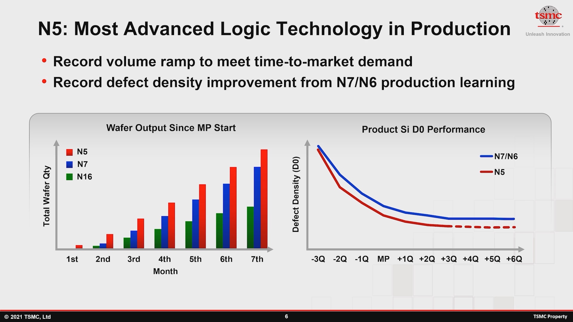
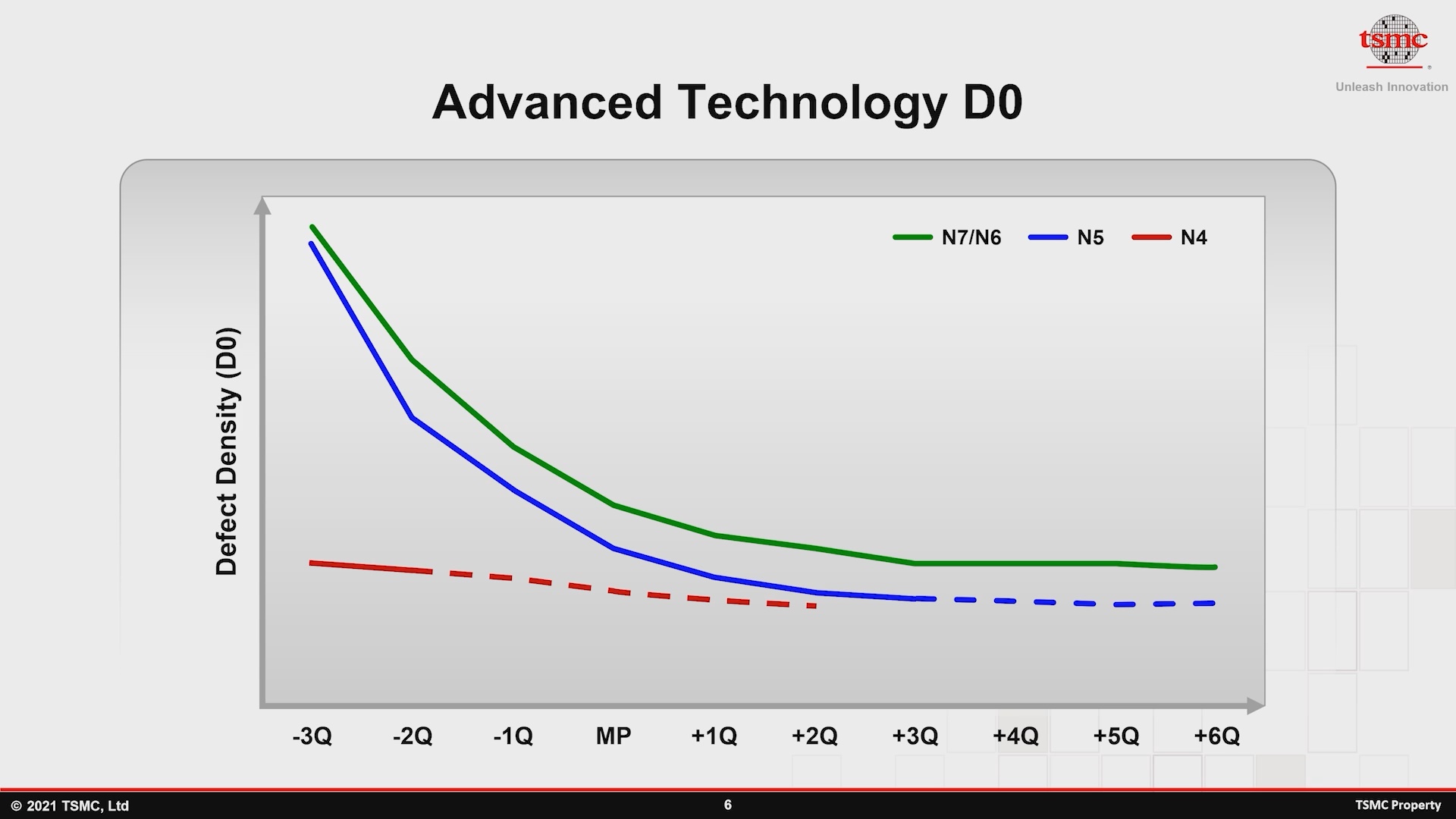
TSMC’s N5 ramp is going extremely well, and as reported back at last year’s Technology Symposium, has reached better yields than the 7nm family process technology nodes ever have. The company here largely points out to simplified manufacturing steps thanks to more extensive usage of EUV layers compared to its 7nm DUV and EUV nodes. In an industry where the competition is struggling to ramp up yields on the latest leading-edge nodes, this is truly an astonishing feat by TSMC which should further cement the foundry’s current dominance.
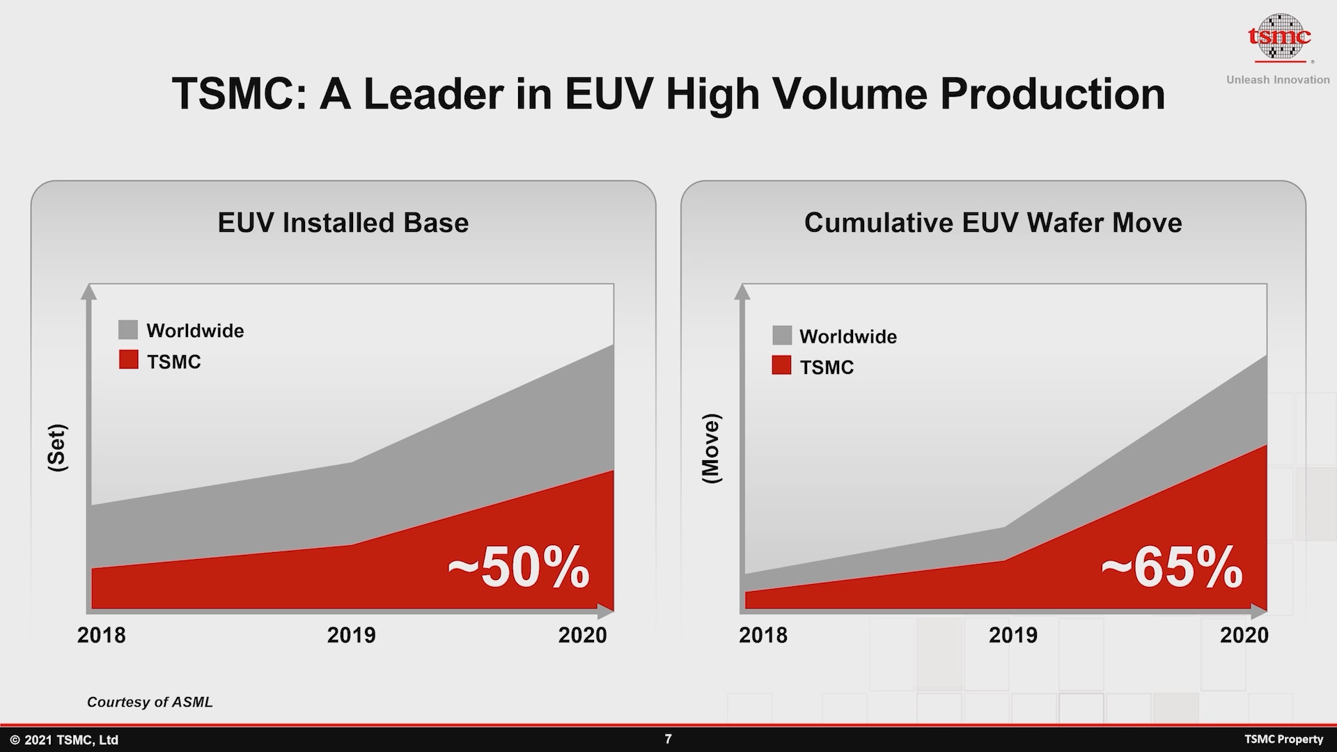
The foundry is well aware of this fact and proudly demonstrates its technical prowess through an extremely interesting metric: Although TSMC “only” has 50% of the worldwide EUV machine install base, the company actually represents 65% share of the cumulative shipped EUV wafers, meaning that it’s making much more effective usage of its install capacity.
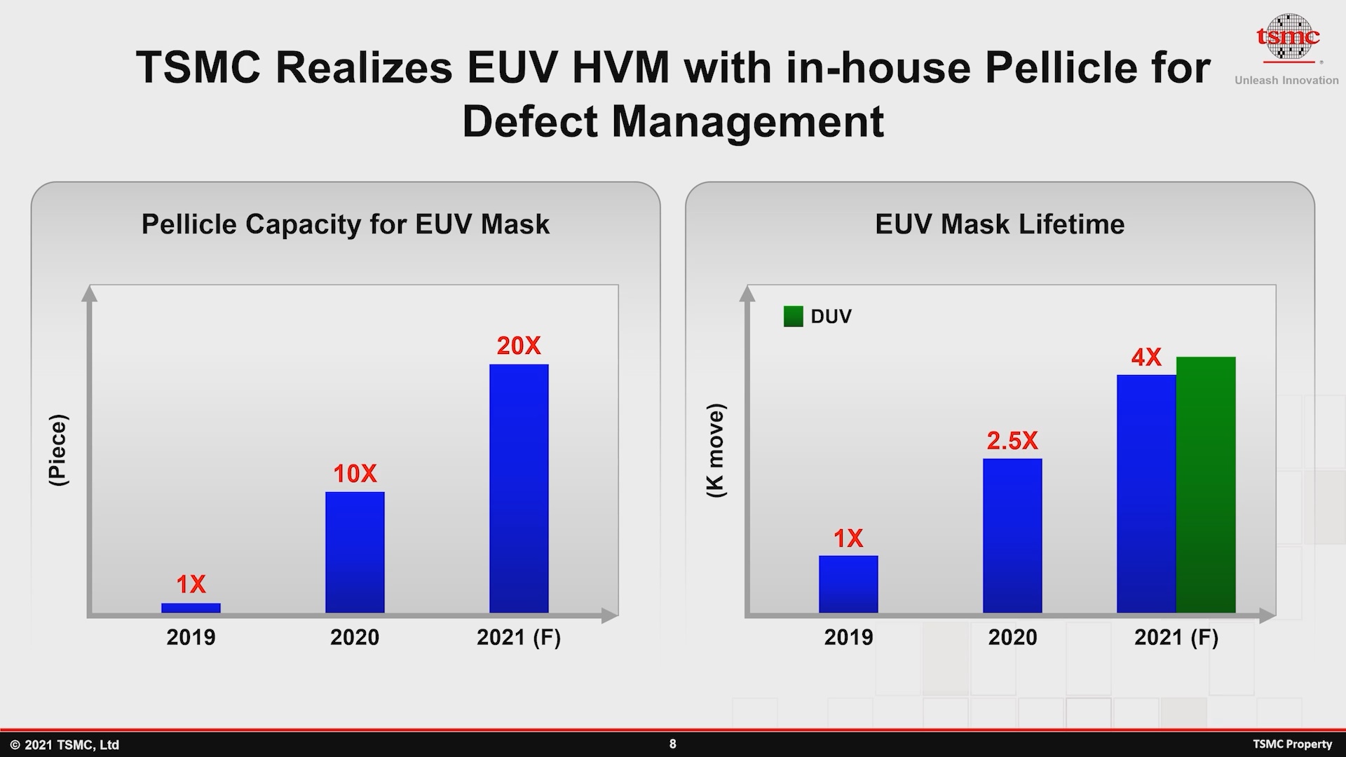
TSMC states that it’s been using an in-house developed pellicle for its EUV nodes since 2019 and more extensively in 2020. In comparison, ASML and Mitsui Chemicals only had recently a few months ago announced that they’re only planning to start volume sales of their own pellicle in 2Q21, essentially right now at the time of this article (ASML has reached out to us to clarify that they've been shipping pellicles to customers in volume for two years - thousands of units from their own production lines, and that the deal with Mitsui is solely transferring that volume production line externally). TSMC doesn’t state any technical details of their in-house pellicle, but if the N5 yields are to be a sign of the results, then it must be an important part of TSMC’s current success at leading edge nodes.
The company also noted that it’s been continuously improving EUV mask lifetime – meaning the amount of time that a mask is useable before it has to be replaced or repaired, pointing out that it is forecasting that it will roughly catch up with DUV mask lifetimes in 2021. In other words, it means that up until now, EUV masks had notably worse lifetime that would result in less manufacturing throughput due to downtime.
N4: Small Optical Shrink of N5
TSMC’s N4 node is a rather straightforward migration path from N5, leveraging iterative improvements in the process.
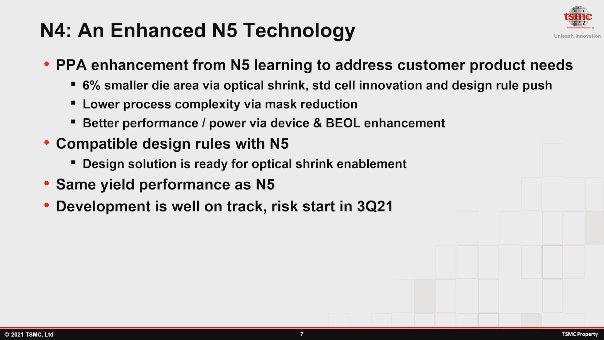
The company states that N4 promises a 6% density improvement over N5, achieved through optical shrinks of the logic, std cell library improvements and design rule pushes for tighter area usage. It’s stated that we’ll be seeing lower manufacturing process complexity through the reduction of masks, although not detailing the exact changes.
N4 representing smaller iterative changes has the benefit that yields are essentially roughly picking up where N5 is currently tracking at. This fact, along with the simplified process complexity would largely indicate that the N4 could well represent a similar shift from N5 that N6 currently is undergoing over N7, with many customers shifting over the new improved node.
We'll be covering more about TSMC's 2021 Technology Symposium in the coming days as we get to write things up, including more details on N3 and future nodes such as N2 and beyond - so please stay tuned.
Related Reading:
- TSMC Update: 2nm in Development, 3nm and 4nm on Track for 2022
- TSMC Q1 2021 Process Node Revenue: More 7nm, No More 20nm
- TSMC to Spend $100B on Fabs and R&D Over Next Three Years: 2nm, Arizona Fab & More
- 3DFabric: The Home for TSMC’s 2.5D and 3D Stacking Roadmap
- TSMC: We have 50% of All EUV Installations, 60% Wafer Capacity
- Where are my GAA-FETs? TSMC to Stay with FinFET for 3nm


50 Comments
View All Comments
mode_13h - Wednesday, June 2, 2021 - link
> such as wafersI mean substrate, but I can imagine there are other upstream inputs also in short supply.
Gondalf - Wednesday, June 2, 2021 - link
Agreed N5 have better yields thanks to EUV but what about output ??The EVU scanners are really slow and not much reliable, so at the end N5 is a big problem for many. No volume
N7 will remain the dominant process for a lot.
The huge delay of AMD Zen 4 (only sometime in H2/2022 or early 2023) is something to think about. Cause process concerns now AMD is at a two years refresh from a steady one year (or little more) refresh
Smell This - Wednesday, June 2, 2021 - link
Gondaft and his trolling FUD have become a stable here, at AT.
Thanks for playing. We enjoy your swings, and misses, and look forward to your future mind-bending gyrations and contortions of the truth ...
Gondalf - Wednesday, June 2, 2021 - link
The realty is worse than dreams Smell. You trust too much in Foundries claims.mode_13h - Wednesday, June 2, 2021 - link
So, what do you trust too much in?Qasar - Wednesday, June 2, 2021 - link
no, your reality is worse, and you trust to much in anything intel tells youmelgross - Wednesday, June 2, 2021 - link
This doesn’t seem to get true at all. TSMC is working capacity. There is so much demand they haven’t been able to meet, some manufacturers are having their parts built on the inferior Samsung process. By the end of this year, n5 will catch up to n7, and by mid next year, bypass it.smalM - Friday, June 4, 2021 - link
N5 capacity will grow to 120k wpm and that's it. There is a reason, TSMC want's to built a fourth Phase for N5, but even TSMC and Dacin will need two years for the realisation.N7 capacity already reached 140k wpm by the end of 2020 and is still expanded.
eastcoast_pete - Wednesday, June 2, 2021 - link
That bit about TSMC using their own pellicles for EUV since 2019 is indeed interesting; EUV scanners apparently either require especially hard UV radiation-resistant pellicles, use them up faster, or both. Thus, as TSMC has their own, home made pellicles, and if those are better than third party ones are, that would go some way to explain why TSMC has better EUV processes and yields than, let's say, Samsung's foundries.Anymoore - Saturday, June 5, 2021 - link
Found that interesting too. One has to wonder where Samsung is as far as pellicles are concerned.TSMC's pellicle talk does conflict a previous brag: https://esg.tsmc.com/csr/en/update/greenManufactur...