Imagination Announces B-Series GPU IP: Scaling up with Multi-GPU
by Andrei Frumusanu on October 13, 2020 4:00 AM EST- Posted in
- GPUs
- Imagination Technologies
- SoCs
- IP
Configurations - Up to 4 GPUs at 6TFLOPs
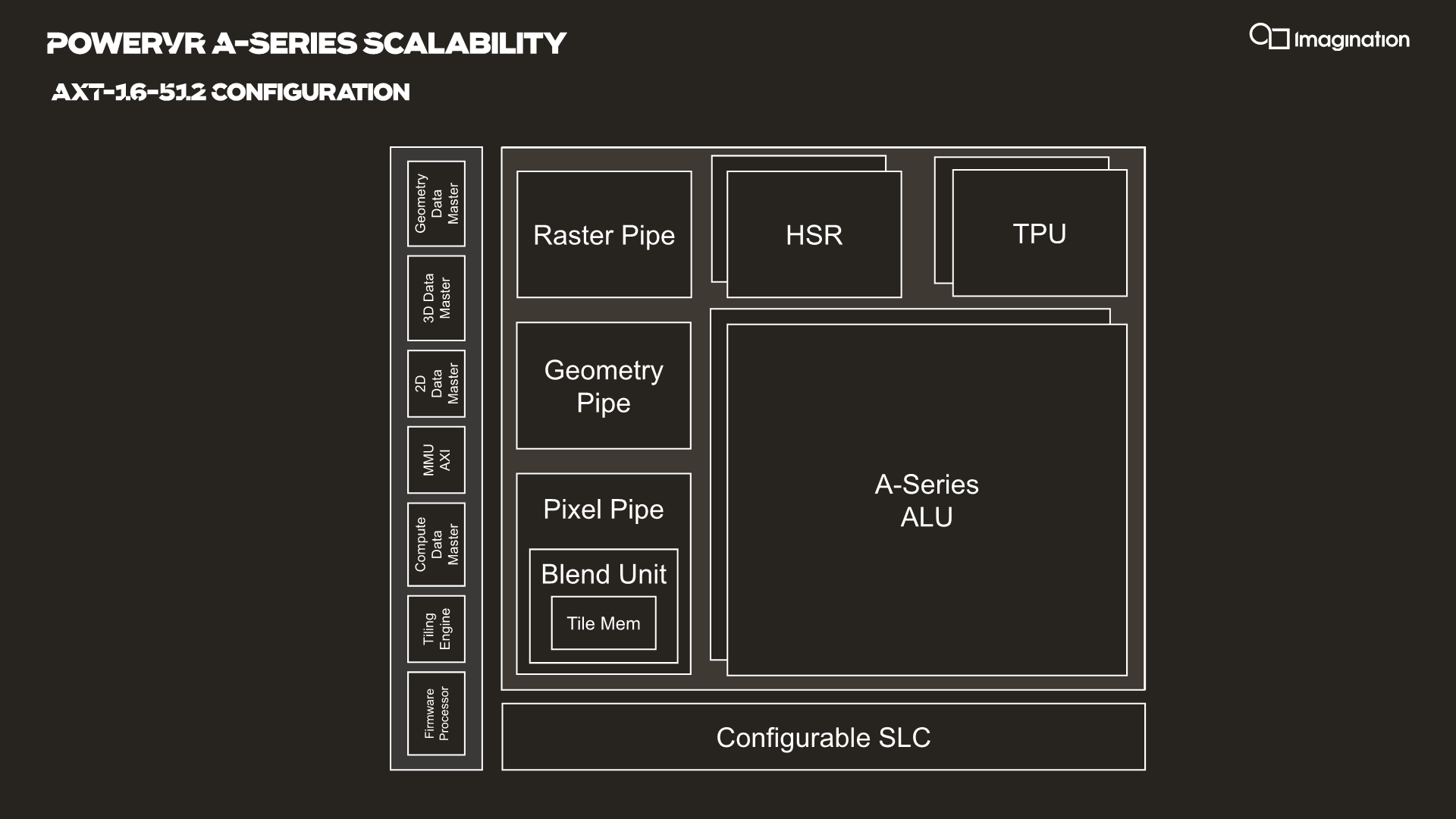
Starting off with the smallest GPU building blocks, it’s good to remind ourselves how an Imagination GPU looks like – the following is from last year’s A-Series presentation:
| PowerVR GPU Comparison | ||||
| AXT-16-512 BXT-16-512 |
GT9524 | GT8525 | GT7200 Plus | |
| Core Configuration |
1 SPU (Shader Processing Unit) - "GPU Core" 2 USCs (Unified Shading Clusters) - ALU Clusters |
|||
| FP32 FLOPS/Clock MADD = 2 FLOPs MUL = 1 FLOP |
512 (2x (128x MADD)) |
240 (2x (40x MADD+MUL)) |
192 (2x (32x MADD+MUL)) |
128 (2x (16x MADD+MADD)) |
| FP16 Ratio | 2:1 (Vec2) | |||
| Pixels / Clock | 8 | 4 | ||
| Texels / Clock | 16 | 8 | 4 | |
| Architecture | A-Series B-Series |
Series-9XTP (Furian) |
Series-8XT (Furian) |
Series-7XT (Rogue) |
Fundamentally and at a high-level, the new B-Series GPU microarchitecture looks very similar to the A-Series. Microarchitecturally, Imagination noted that we should generally expect a 15% increase in performance or increase in efficiency compared to the A-Series, with the building blocks of the two GPU families being generally the same save for some more important additions such as the new IMGIC (Imagination Image Compression) implementation which we’ll cover in a bit.
An XT GPU still consists of the new SPU design which houses the new more powerful TPU (Texture Processing Unit) as well as the new 128-wide ALU designs that is scaled into ALU clusters called USCs (Unified Shading Clusters).
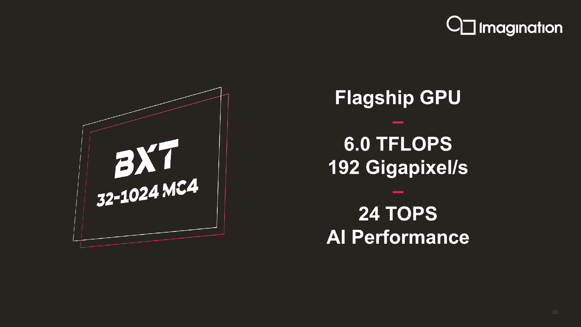
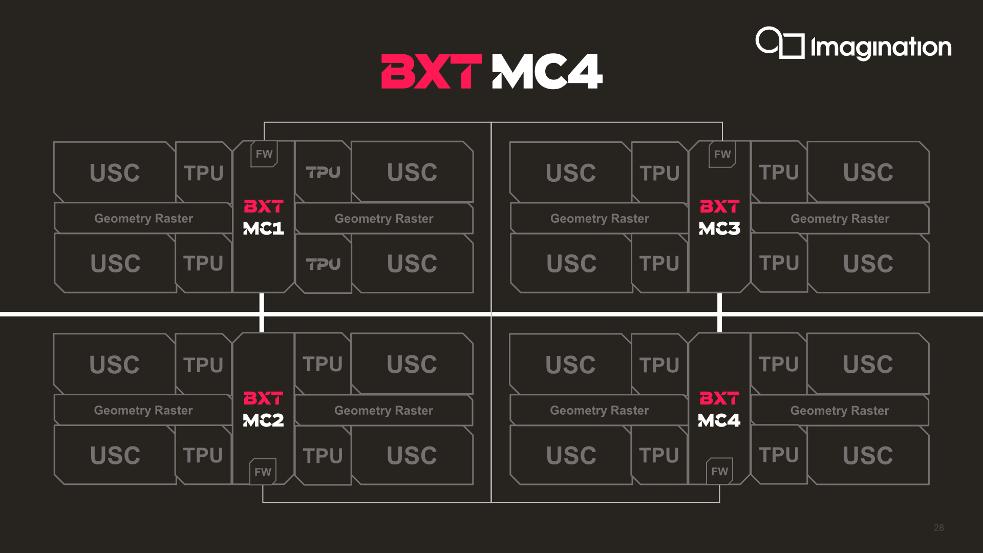
Imagination’s current highest-end hardware implementation in the BXT series is the BXT 32-1024, and putting four of these together creates an MC4 GPU. In a high-performance implementation reaching up to 1.5GHz clock speeds, this configuration would offer up to 6TFLOPs of FP32 computing power. Whilst this isn’t quite enough to catch up to Nvidia and AMD, it’s a major leap for a third-party GPU IP provider that’s been mostly active in the mobile space for the last 15 years.

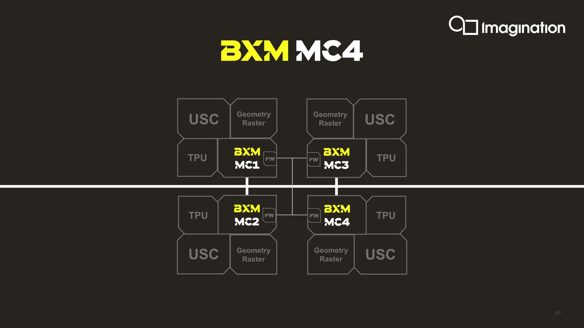
The company’s BXM series continues to see a differentiation in the architecture as some of its implementations do not use the ultra-wide ALU design of the XT series. For example, while the BXM-8-256 uses one 128-wide USC, the more area efficient BXM 4-64 for example continues to use the 32-wide ALU from the 8XT series. Putting four BXM-4-64 GPUs together gets you to a higher performance tier with a better area and power efficiency compared to a larger single GPU implementation.
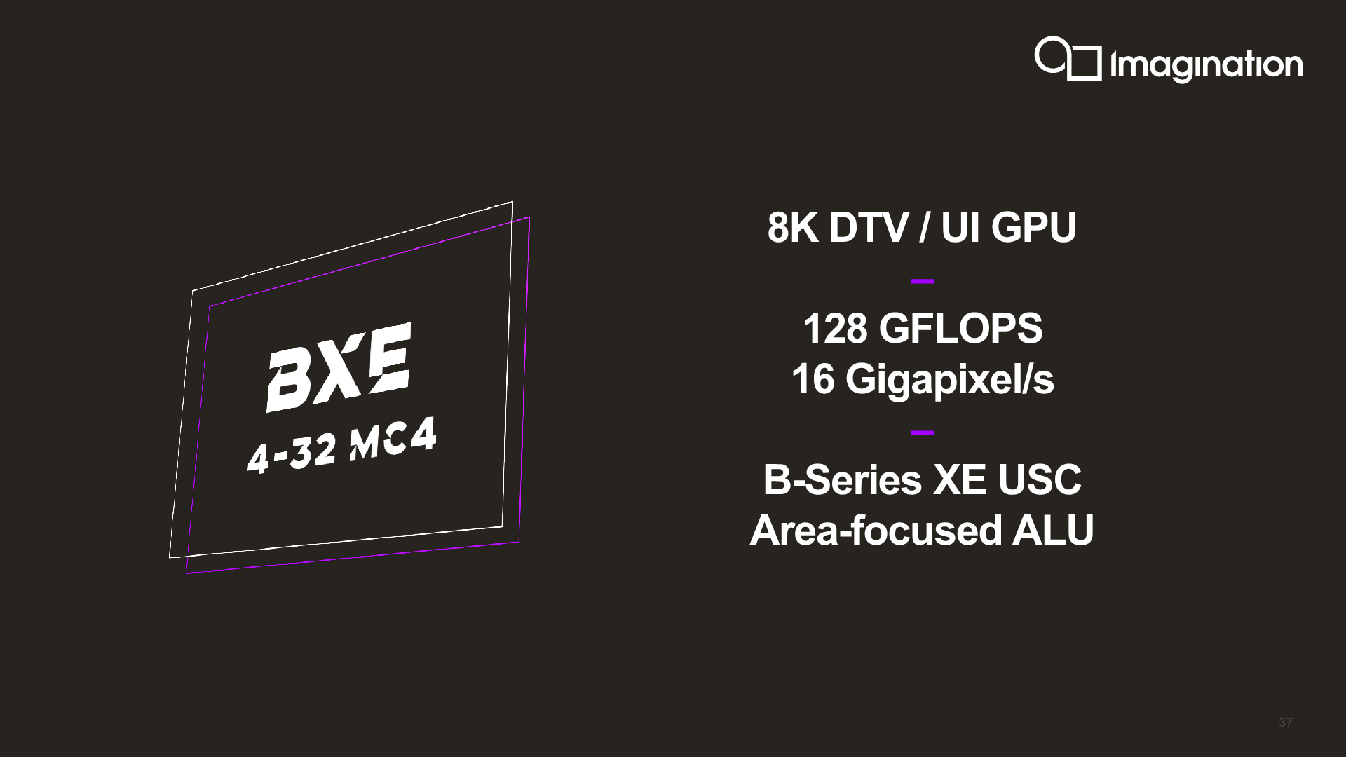
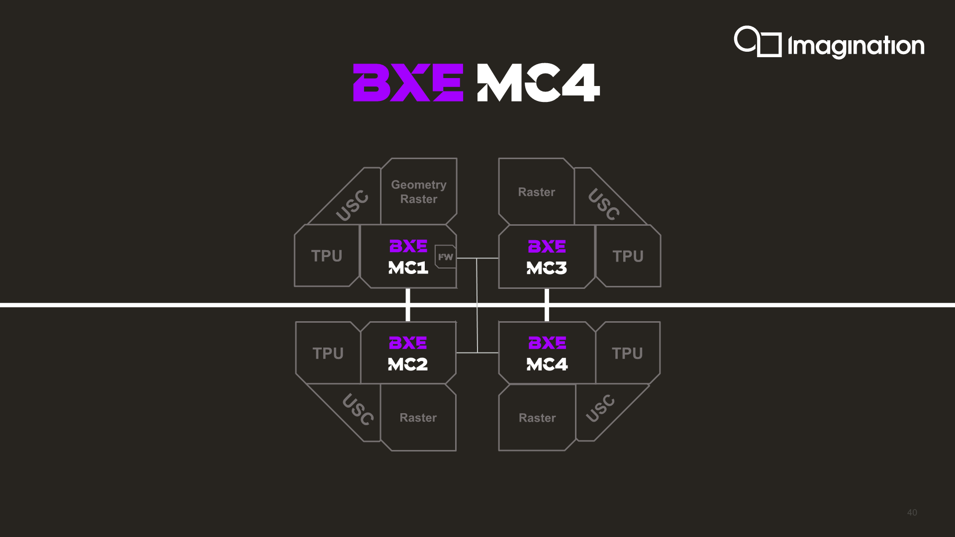
The most interesting aspect of the multi-GPU approach is found in the BXE series, which is Imagination’s smallest GPU IP that purely focuses on getting to the best possible area efficiency. Whilst the BXT and BXM series GPUs until now are delivered as “primary” cores, the BXE is being offered in the form of both a primary as well as a secondary GPU implementation. The differences here is that the secondary variant of the IP lacks a firmware processor as well as a geometry processing, instead fully relying on the primary GPU’s geometry throughput. Imagination says that this configuration would be able to offer quite high compute and fillrate capabilities in extremely minuscule area usage.
| PowerVR Hardware Designs GPU Comparison | ||||||
| Family | Texels/ Clock |
FP32/ Clock |
Cores | USCs | Wavefront Width |
MC Design |
| BXT-32-1024 MC1 | 32 | 1024 | 1 | 4 | 128 | P |
| BXT-16-512 MC1 | 16 | 512 | 1 | 2 | 128 | P |
| BXM-8-256 MC1 | 8 | 256 | 1 | 1 | 128 | P |
| BXM-4-64 MC1 | 4 | 64 | 1 | 1 | 32 | P |
| BXE-4-32 Secondary | 4 | 32 | 1 | 1 | 16 | S |
| BXE-4-32 MC1 | 4 | 32 | 1 | 1 | 16 | P |
| BXE-2-32 MC1 | 2 | 32 | 1 | 1 | 16 | P |
| BXE-1-16 MC1 | 1 | 16 | 1 | 1 | 8 | P |
Putting the different designs into a table, we’re seeing only 8 different hardware designs that Imagination has to create the RTL and do physical design and timing closure on. This is already quite a nice line-up in terms of scaling from the lowest-end area focused IP to something that would be used in a premium high-end mobile SoC.
| PowerVR MC GPU Configurations | ||||||
| Family | Texels/ Clock |
FP32/ Clock |
Cores | USCs | Wavefront Width |
MC Design |
| BXT-32-1024 MC4 | 128 | 4096 | 4 | 16 | 128 | PPPP |
| BXT-32-1024 MC3 | 96 | 3072 | 3 | 12 | 128 | PPP |
| BXT-32-1024 MC2 | 64 | 2048 | 2 | 8 | 128 | PP |
| BXT-32-1024 MC1 | 32 | 1024 | 1 | 4 | 128 | P |
| BXT-16-512 MC1 | 16 | 512 | 1 | 2 | 128 | P |
| BXM-8-256 MC1 | 8 | 256 | 1 | 1 | 128 | P |
| BXM-4-64 MC4 | 16 | 256 | 4 | 4 | 32 | PPPP |
| BXM-4-64 MC3 | 12 | 192 | 3 | 3 | 32 | PPP |
| BXM-4-64 MC2 | 8 | 128 | 2 | 2 | 32 | PP |
| BXM-4-64 MC1 | 4 | 64 | 1 | 1 | 32 | P |
| BXE-4-32 MC4 | 16 | 128 | 4 | 4 | 16 | PSSS |
| BXE-4-32 MC3 | 12 | 96 | 3 | 3 | 16 | PSS |
| BXE-4-32 MC2 | 8 | 64 | 2 | 2 | 16 | PS |
| BXE-4-32 MC1 | 4 | 32 | 1 | 1 | 16 | P |
| BXE-2-32 MC1 | 2 | 32 | 1 | 1 | 16 | P |
| BXE-1-16 MC1 | 1 | 16 | 1 | 1 | 8 | P |
The big flexibility gain for Imagination and their customers is that they can simple take one of the aforementioned hardware designs, and scale these up seamlessly by laying out multiple GPUs. On the low-end, this creates some very interesting overlaps in terms of compute abilities, but offer different fillrate capabilities at different area efficiency options.
At the high-end, the biggest advantage is that Imagination can quadruple their processing power from their biggest GPU configuration. Imagination notes that for the BXT series, they no longer created a single design larger than the BXT-32-1024 because the return on investment would simply be smaller, and involve more complex timing work than if a customer would simply scale performance up via a multi-core implementation.


74 Comments
View All Comments
AMDSuperFan - Tuesday, October 13, 2020 - link
I would like to see some benchmarks of this product against Big Navi to help me make a good decision. So far, nothing seems to measure up.myownfriend - Tuesday, October 13, 2020 - link
The only places where it could really compare with Big Navi is if there's a game with a lot of overdraw that a maxed out B-series GPU would be able to rid itself of.persondb - Tuesday, October 13, 2020 - link
Honestly, I am not fully understanding as to how this GPU is supposed to compete in the high perfomance computing market. AFAIK, that market is hungry for tflops(as well as fast memory) yet this does not seem to deliver enough tflops.In fact, it's very disappointing specially for the tradeoffs that you would be forced to do in a multi-chiplet design. There are also a bunch of design decisions, that seem like they would hurt latency and possibly performance as well.
The article mentions that it has two possible configurations, one where a 'primary' GPU works as a 'firmware processor' to divide the workload across the other GPUs, in that kind of thing, it would seem to me that it would add some latency and overhead over the more traditional GPU. While the other configuration lacks a firmware processor but is completely limited by the primary GPU geometry unit.
Funnily enough, it don't seem like they have provided any detail about the memory controllers nor about the cache, possibly because it would be obvious that such a configuration would have it's severe tradeoff? There is also nothing about the interconnect that would link the GPUs together, this is an important one as it can have great impacts on the latency. You need to have them have some data sharing unless each GPU would only utilize the data it can get through it's own memory controller, but that could lead to problems too.
There are a bunch of things there that can increase latency and hamper performance. I personally would be skeptical about this until it releases and there are information on how this actually goes.
myownfriend - Wednesday, October 14, 2020 - link
This design is not forcing anybody to go with chiplets. These multiple GPUs can be placed on one chip. As far as peak TFLOPS and fast memory, my guess is that you aren't familiar with tile-based rendering, specifically Imagination's Tile-Based Deferred Renderer, does.AMD or Nvidia GPUs just pull vertices from external memory, then transform, rasterize, and fragment shade them then writing them back to external memory. All color and depth reads and writes happen in external memory. To make the most of that memory bandwidth and shader performance, game designers need to sort draw calls from near to far and maybe do a depth pre-pass to get rid of overdraw though there there will also be overdraw that occurs per draw call.
A tile based GPU pulls vertices from external memory then transforms them into screen space, clips and culls them, then write them back out into external memory as compressed bins that represent different tiles on the screen. It then reads them back a few tiles at a time and applies hidden surface removal on opaque geometry to remove overdraw completely. That process creates an on-chip depth/stencil buffer which insures that only pixels that contribute the final image get submitted for fragment shading. It then attempts to create the back-buffer for that tile completely within a small amount of on-chip color buffer memory so that it only needs to write back the finalized tile to external memory.
The depth buffer never even has to get written to external memory, all overdraw for opaque geometry is completely removed regardless of the order they were submitted to the GPU, and the 6TFLOPs that the B series can theoretically achieve is being spread among fewer pixels. It has far less reliance on external memory bandwidth since it only really needs to use it read textures and geometry data and store the tile list. Since on-chip memory can potentially use very high bus widths and run in-sync with the GPU, they could easily provide more bandwidth than GDDR6X memory. At 1500Mhz with four GPUS and four tiles per GPU, a 256-bit bus to each tile would feed it with 768GB/s of low-latency memory bandwidth. If you're curious how large each tile is, previous Imagination GPUs used 32x32 pixel tiles or smaller so a 256-bit G-buffer would only require about 32KB per tile so it can just use SRAM.
That tiling process also provides a simple way of dividing up the work among the GPUs. You mentioned that configuration that uses a primary GPU. The article says that would be the only one with a firmware processor and a geometry front end so it would be the one that handles all vertex processing and tiling but after those tiles are written to main-memory, the only communication that it needs to make with other GPUs is to tell them to read some of those tiles. They can then work almost completely independently from each other.
To my knowledge, even per compute workloads can take advantage of those on-chip buffers as a kind of scratchpad RAM.
Threska - Wednesday, October 14, 2020 - link
I remember this discussion with my Apocalypse and PowerVR. Shame the idea never really took hold.persondb - Friday, October 16, 2020 - link
Modern GPUs since Vega and Maxwell already use a hybrid of tile based rendering and more traditional rendering methods(you can see this old-ish video on nvidia approach https://www.youtube.com/watch?v=Nc6R1hwXhL8). IDK why you commented on it. Since that means it's not a straight comparison of Tiled vs traditional methods.I mentioned TFLOPs for compute workloads and not those graphical workloads, which was described in the article as being one of the potential markets for this. As far as I am aware, a gpu that is tile based wouldn't change much for pure compute workloads.
Also about that memory, I really doubt with that kind of configuration the latency would be that low. Probably higher than you expect. Though of course, GPUs generally aren't latency sensitive as CPUs. But it's also not that much higher than something with GDDR6X(or just GDDR6 with some 16 gbps chips).
I must say that I am not familiar with tile based GPUs, but say per example about textures. Obviously you need to get them from the external memory, as there is no SRAM in the world that could store all textures that you need. This would obviously complicate the memory controller issue as I was talking about in my original post. Same for say computing with large memory requirement.
Obviously, if each of the chiplet has their own (say 64-bit) memory controller then they will need an interconnect to share the data. And that is what I was talking about, such a thing would increase latency. And again, the article does not say how the memory controllers are set up for those chiplets.
myownfriend - Friday, October 16, 2020 - link
Tiled caching and tile-based rendering are still very different. Tiled caching can't do that and I believe it only works on a small buffer of geometry at a time as it works completely within the 2MB of L2 cache which is not enough to store the geometry for a whole scene. It's enough to have reduced the required external memory bandwidth by quite a bit. Tile-based rendering creates the primitive/parameter buffer in external memory before pulling them back on chip tile by tile and has the ability to create the entire back-buffer for each tile completely within on-chip memory.https://www.imgtec.com/blog/a-look-at-the-powervr-...
In modern games, textures and geometry take up a lot of space in RAM but account for very little of the used memory bandwidth. Textures are generally compressed to 4 bits per pixel (though ASTC allows bit rates from 8 to 0.89 bits per pixel) and are read once to a few times at the beginning of the frame. The majority of bandwidth is needed for the back buffer which, for an Ultra HD game with a 256-bit G-buffer, would only take up about 265 MBs of space but would be written to and read from multiple times per-pixel per-frame. That's why the Xbox One had 32MB of ESRAM with a max bandwidth of 205-218GB/s and 8GB of DDR3 over a 256-bit bus with only 68.3GB/s of bandwidth. The ESRAM was large enough to store a 128-bit 1080p g-buffer and the DDR3 stores textures and geometry and acts as work RAM for the CPU. If a game has low-quality textures these days, it's generally blamed on the amount of RAM not its speed. As resolution increases, the average texture samples per-pixel goes down. In other words, if the chiplets do need to fetch texture samples from each other then it wouldn't require all that much chiplet to chiplet bandwidth. Using that XBO as an example, that's 17.075 GB/s per 64-bit memory controller without accounting for the fact that the CPU is using some of that. That's 40% of the die to die bandwidth between AMD's Zeppelin chiplets. TBDR would decrease texture bandwidth even more because it only fetches texels for visible fragments.
I'm not sure what you mean by "Also about that memory, I really doubt with that kind of configuration the latency would be that low. Probably higher than you expect." Are you talking about how said that the on-chip memory is ultra low-latency and high bandwidth? Because it would absolutely be low-latency. We're talking about a very local pool of SRAM that's running at the same clock as the ALUs. Meanwhile GDDR6X would have to be accessed via requests from memory controllers that are being shared by the whole chip then traveling off-package, through the motherboard and then into a separate package and back.
You're right about compute workloads not being all that different between TBRs and IMRs so a compute load that generally needs a lot of high bandwidth memory would still have the same requirements for external memory. However, I'm lead to believe that the reason GPUs are used for compute workloads is because those compute workloads, like graphics workloads, are considered embarrassingly parallel so I don't really know how much data moves horizontally in the GPU. It is very possible that most GPU compute workloads could be modified to make some use of the on-chip storage to reduce reliance on external memory.
I'm also curious to see how those memory controllers are set up, too, but I'm a bit more confident in a TBRs ability to scale in a multi-GPU set up.
myownfriend - Wednesday, October 14, 2020 - link
The last time Imagination's GPUs were in the desktop space was in 2001 with the Kyro II. GPUs then and now are very different but this article can still give you a sense of what sort of gains a TBDR GPU could potentially provide.https://www.anandtech.com/show/735/10
Compared to the Geforce2 Ultra, the Kyro II used under half the amount of transistors, under half the power, had 36% of the memory bandwidth, 35% of the fill rate, and cost 44% of the price yet it actually beat the Geforce2 Ultra in some tests especially at higher resolutions.
eastcoast_pete - Wednesday, October 14, 2020 - link
One area currently grossly underserved by both NVIDIA and AMD is in entry-level dGPUs with decent ASICs for HEVC/h265, VP9 and AV1 decode in 10bit HDR/HDR+ on board. Basically, PCIe cards with 2-4 Gb VRAM under $ 100 that still beat the iGPUs in Renoirs and Tiger Lakes (Xe). That market is up for grabs now, maybe these GPUs can fill that void?vladx - Wednesday, October 14, 2020 - link
Video encode/decode is one of the features used by cloud GPUs so it would most likely be able to do all that.