Micron Spills on GDDR6X: PAM4 Signaling For Higher Rates, Coming to NVIDIA’s RTX 3090
by Ryan Smith on August 20, 2020 12:00 PM EST
It would seem that Micron this morning has accidentally spilled the beans on the future of graphics card memory technologies – and outed one of NVIDIA’s next-generation RTX video cards in the process. In a technical brief that was posted to their website, dubbed “The Demand for Ultra-Bandwidth Solutions”, Micron detailed their portfolio of high-bandwidth memory technologies and the market needs for them. Included in this brief was information on the previously-unannounced GDDR6X memory technology, as well as some information on what seems to be the first card to use it, NVIDIA’s GeForce RTX 3090.
The document seems to have been posted a month (or more) early, given the mention of the NVIDIA card, which we’re not expecting to be announced any sooner than at NVIDIA’s September event. Furthermore the document links to other, still-unpublished Micron technical briefs involving GDDR6X. None the less, the document does come directly from Micron’s public webservers, so what we have today is an unexpected sneak peek at Micron's upcoming GDDR memory plans.
At any rate, as this is a market overview rather than a technical deep dive, the details on GDDR6X are slim. The document links to another, still-unpublished document, “Doubling I/O Performance with PAM4: Micron Innovates GDDR6X to Accelerate Graphics Memory”, that would presumably contain further details on GDDR6X. None the less, even this high-level overview gives us a basic idea of what Micron has in store for later this year.
Update 8/20: Micron has since published (and removed) the second GDDR6X document. By and large it confirms our expectations for the GDDR6X technical specifications that weren't in Micron's original document. More information is available below.
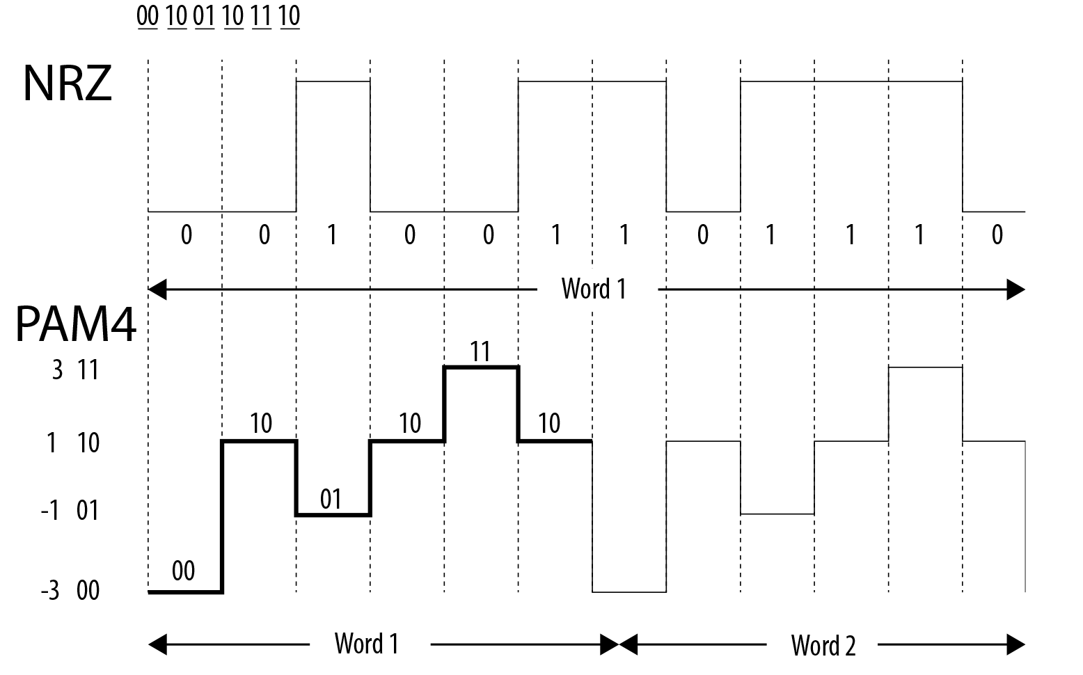
The key innovation for GDDR6X appears to be that Micron is moving from using NRZ coding on the memory bus – a binary (two state) coding format – to four state coding in the form of Pulse-Amplitude Modulation 4 (PAM4). In short, Micron would be doubling the number of signal states in the GDDR6X memory bus, allowing it to transmit twice as much data per clock.
| GPU Memory Math | ||||||
| GDDR6X (RTX 3090) |
GDDR6 (Titan RTX) |
GDDR5X (Titan Xp) |
HBM2 (Titan V) |
|||
| Total Capacity | 12 GB | 12 GB | 12 GB | 12 GB | ||
| B/W Per Pin | 21 Gbps | 14 Gbps | 11.4 Gbps | 1.7 Gbps | ||
| Chip capacity | 1 GB (8 Gb) | 1 GB (8 Gb) | 1 GB (8 Gb) | 4 GB (32 Gb) | ||
| No. Chips/KGSDs | 12 | 12 | 12 | 3 | ||
| B/W Per Chip/Stack | 84 GB/s | 56 GB/s | 45.6 GB/s | 217.6 GB/s | ||
| Bus Width | 384-bit | 384-bit | 352-bit | 3072-bit | ||
| Total B/W | 1008 GB/s | 672 GB/s | 548 GB/s | 652.8 GB/s | ||
| DRAM Voltage | 1.35 V | 1.35 V | 1.35 V | 1.2 V | ||
| Data Rate | QDR | QDR | DDR | DDR | ||
| Signaling | PAM4 | Binary | Binary | Binary | ||
PAM4 itself is not a new technology, and has been used in other high-end devices like network transceivers well before now. More recently, the PCI-SIG announced that they’d be adopting PAM4 coding for PCIe 6.0. So for a slightly more detailed discussion on PAM4, here is our explaination from our PCIe 6.0 primer:
At a very high level, what PAM4 does versus NRZ (binary coding) is to take a page from the MLC NAND playbook, and double the number of electrical states a single cell (or in this case, transmission) will hold. Rather than traditional 0/1 high/low signaling, PAM4 uses 4 signal levels, so that a signal can encode for four possible two-bit patterns: 00/01/10/11. This allows PAM4 to carry twice as much data as NRZ without having to double the transmission bandwidth, which for PCIe 6.0 would have resulted in a frequency around 30GHz(!).
NRZ vs. PAM4 (Base Diagram Courtesy Intel)
PAM4 itself is not a new technology, but up until now it’s been the domain of ultra-high-end networking standards like 200G Ethernet, where the amount of space available for more physical channels is even more limited. As a result, the industry already has a few years of experience working with the signaling standard, and with their own bandwidth needs continuing to grow, the PCI-SIG has decided to bring it inside the chassis by basing the next generation of PCIe upon it.
The tradeoff for using PAM4 is of course cost. Even with its greater bandwidth per Hz, PAM4 currently costs more to implement at pretty much every level, from the PHY to the physical layer. Which is why it hasn’t taken the world by storm, and why NRZ continues to be used elsewhere. The sheer mass deployment scale of PCIe will of course help a lot here – economies of scale still count for a lot – but it will be interesting to see where things stand in a few years once PCIe 6.0 is in the middle of ramping up.
Thus far, PAM4 signaling has only been used for networking and expansion buses, so using it for a memory bus, though a logical extension, would represent a big leap in technology. Now Micron has to develop memory that can not only do clean PAM4 modulation – which is not a simple task – but NVIDIA needs a matching memory controller on the other end. It’s doable, and probably inevitable, but it’s a big change from how memory buses have traditionally operated – even high-speed buses like those used for GDDR.
According to Micron’s brief, they’re expecting to get GDDR6X to 21Gbps/pin, at least to start with. This is a far cry from doubling GDDR6’s existing 16Gbps/pin rate, but it’s also a data rate that would be grounded in the limitations of PAM4 and DRAM. PAM4 itself is easier to achieve than binary coding at the same total data rate, but having to accurately determine four states instead of two is conversely a harder task. So a smaller jump isn’t too surprising.
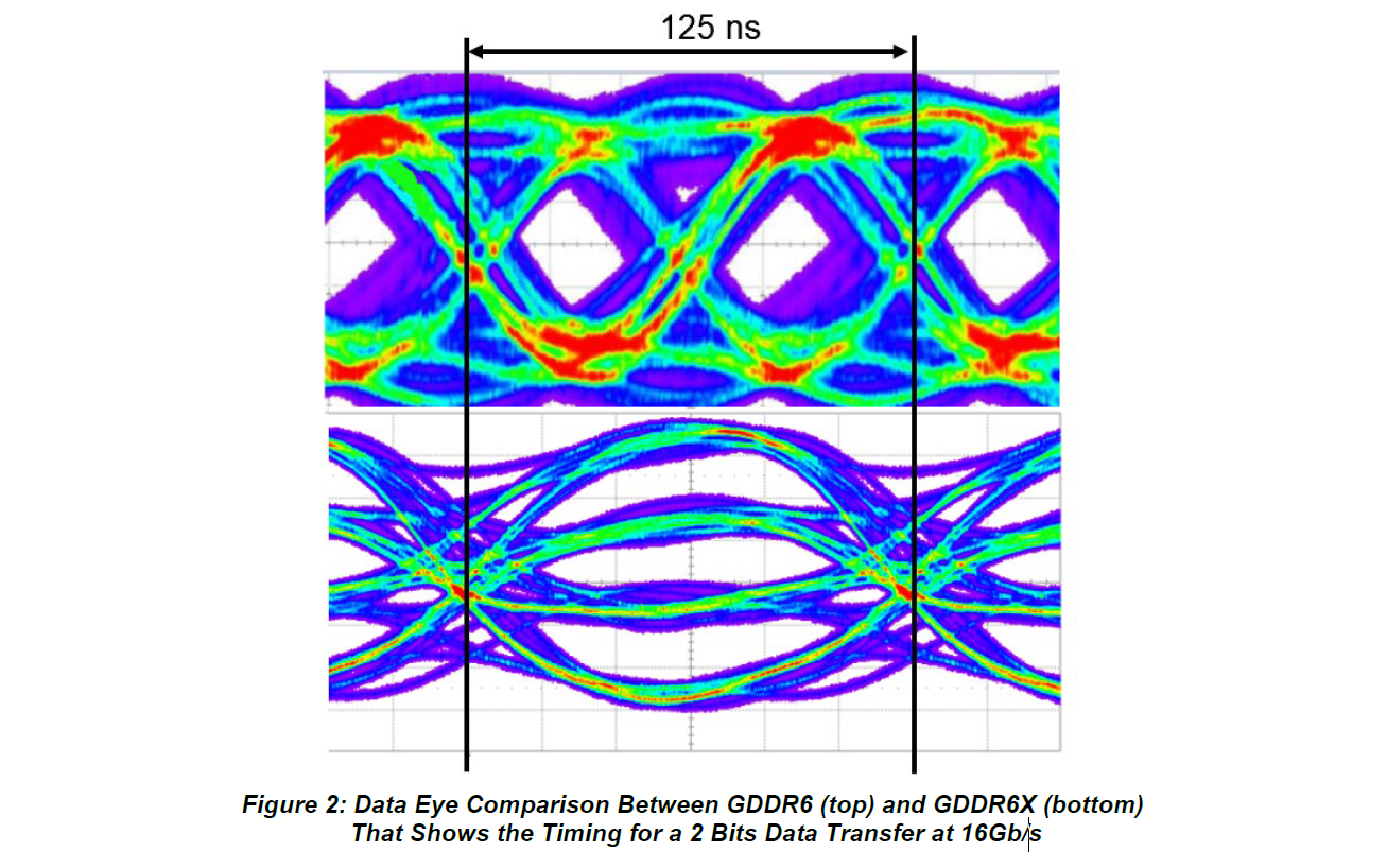
Ultimately, PAM4 is a means of trading signal-to-noise tolerances for greater bandwidth. Decoding among 4 states instead of 2 requires a very clean and strong signal (just take a look at Micron's PAM4 eye diagram below), but because GDDR6 already has very tight signal requirements due to its high bus frequency, PAM4 doesn't require exceptionally higher SNRs – at least not at more modest data rates. Still, video card makers will be working with a technology that has tighter SNR requirements than any memory technology before it, so expect to see this reflected in board designs, both with regards to memory placement (very closely placed for the shortest traces) and in board design costs.
For that reason alone, video card vendors will likely have separate PCB designs for GDDR6 and GDDR6X designs – it's all but guaranteed that GDDR6X host processors will also support GDDR6 as a fallback option – but GDDR6X's requirements do hint at some flexibility here. It's noteworthy that the new memory uses the exact same package and pin count as GDDR6: a 14mm x 12mm package with a 180 pin BGA interface. At this point it isn't confirmed whether GDDR6X's pin-out is identical to GDDR6's – that information will likely come after NVIDIA's new cards are announced – but I wouldn't be the least bit surprised if that were the case. Especially as Micron's sheets reveal that of those 180 pins, GDDR6X uses the same 70/74 signal pins as GDDR6.
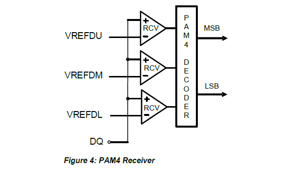
One notable innovation here is that both GDDR6X hosts and memory devices implement now implement sub-receivers in order to achieve the fidelity required to read PAM4 modulation. Each I/O pin gets an Upper, Middle, and Lower receiver, which is used to compare the PAM4 signal against that respective portion of the data eye. So while one signal is still coming in on a pin, it's being viewed by three different receivers to best determine which of the four signal levels it is.
Meanwhile, Micron's second document indicates that the company is going to be pushing the core clocks of their memory a little bit higher than they did GDDR6. As a refresher, DRAM cells more or less flatlined in performance years ago – you can only drive a mixed transistor/capacitor device so quickly – so newer memory technologies have been about ever-greater parallelism. In the case of GDDR technologies, for example, this means that 16Gbps GDDR6 has the same core clock rate as 8Gbps GDDR5.
Based on Micron's documents, it looks like the company intends to achieve a 21Gbps data rate by pushing the core DRAM clockspeed higher. All of their technical comparisons between GDDR6X and GDDR6 show the two running at the same data rates and the same clockspeeds. So we can rule out a GDDR5X-style chance in pre-fetch sizes, as GDDR6X has the same access granularity and burst length (in bits) as GDDR6X.
The major wildcard for the moment is going to be costs. As I mentioned earlier, PAM4 has been around for quite a while; it’s just expensive to use due to the engineering and silicon required. How much will adding PAM4 to a memory chip add to its cost? Clearly this is going to be a premium memory technology, though at the same time it’s a safe bet that Micron wouldn’t be going this route if it was going to cost as much as HBM, which has already become cost-prohibitive for consumer video cards.
Moving on, there’s one final interesting nugget of information on GDDR6X in Micron’s whitepaper, and that’s on power consumption. One of the indirect benefits of PAM4 is that by running a bus at a lower clockrate than would otherwise be required, the power consumption requirements go down. It’s by no means a 2x difference, as PAM4 coding’s complexity eats up power in other ways, but it’s more efficient none the less. And according to Micron, this is going to play out for GDDR6X as well, with GDDR6X having a slightly lower energy cost per bit.
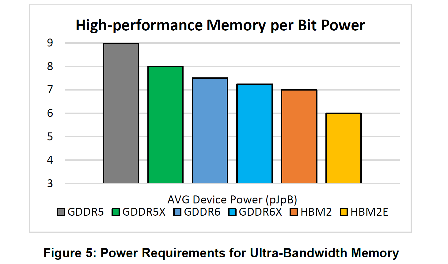
According to Micron's initial brief, we’re looking at an average device power of roughly 7.25 picojoules per byte for GDDR6X, versus 7.5 for GDDR6. Going by this data, this is also relatively close in power efficiency to HBM2, though well behind HBM2E. That said, as this is efficiency per byte, it means that actual power consumption is a function of bandwidth; and while GDDR6X is a little more efficient, it’s slated to be a lot faster.

This is further backed up by Micron's second brief, which offers a power comparison that's normalized to GDDR6. There, Micron states that 21Gbps GDDR6X requires 15% less power per transferred bit than GDDR6 at 14Gbps. But as with Micron's first brief, this is efficiency per byte/bit, not total power consumption. So either way, it's clear that the total power consumption of GDDR6X is going to be higher than today's 14Gbps GDDR6, with Micron projecting 25-27% more power required for 21Gbps GDDR6X memory.
Overall, Micron presents PAM4 as the natural evolution of GDDR memory technology. And while this is wrapped up in obvious technical marketing, there is a nugget of truth, in as much as the official data rates for GDDR6 still top out at 16Gbps. Rambus, for its part, has demonstrated 18Gbps GDDR6 in the labs, but from the outside looking in, it’s not clear right now if that is commercially viable – no memory vendor currently has 18Gbps chips in its catalog.
But regardless of where vanilla GDDR6 eventually tops out at, the memory industry as a larger whole has long been staring down a reckoning with memory bus speeds. Successive standards have employed various techniques to improve data rates, such as GDDR6’s QDR, but GDDR has always remained a single-ended I/O standard using binary coding. With transfer rates per pin now over 16GT/second, one of those two core principles will eventually have to change, as we’ve seen in other fields employing high-speed I/O.

AMD 2011 Technical Forum and Exhibition, Examing Memory Options After GDDR5
PAM4, in turn, is likely to be the lesser of two evils. Throwing out binary coding for PAM4 is, if nothing else, the more energy efficient option. The other route would have been to throw out single-ended I/O for differential signaling, which is something the memory industry is keen to avoid. Differential signaling works, and it works well – GDDR6 even uses it for clocking (and not memory transfers) – but it consumes a lot of pins and even more power. Which is part of the reason that HBM came around. So in one respect PAM4 can be thought as another way to stave off differential signaling on GDDR for at least another generation.
Finally, and while we’re on the subject of memory standards, the conspicuous absence of JEDEC in Micron’s document bears mentioning. The trade organization and standards body is responsible for setting GDDR memory standards, including GDDR6 as well as Micron’s previous attempt at a memory technology offshoot, GDDR5X. Given the premature nature of the brief’s release, it’s not clear whether GDDR6X is another JEDEC standard that is currently being developed privately ahead of a public launch, or if Micron is truly going solo and has developed its own memory standard.
NVIDIA GeForce RTX 3090: 12GB of GDDR6X With Nearly 1TB of Memory Bandwidth?
Last, but not least, let’s talk about the second secret spilled in Micron’s brief, NVIDIA’s GeForce RTX 3090. The presumably high-end video card is apparently Micron’s flagship use case for GDDR6X, and the company has helpfully laid out its typical memory configuration.
In short, according to Micron the video card will ship with 12GB of GDDR6X in a 384-bit memory bus configuration. That memory, in turn, will be clocked at somewhere between 19Gbps and 21Gbps, which at the higher- end of that range would give the card 1008GB/sec of memory bandwidth, just shy of a true 1TB/sec (1024GB/sec) of bandwidth.
| NVIDIA GeForce Specification Comparison | ||||||
| RTX 3090 | RTX 2080 Ti | RTX 2080 | GTX 1080 Ti | |||
| CUDA Cores | Many | 4352 | 2944 | 3584 | ||
| Memory Clock | 19-21Gbps GDDR6X | 14Gbps GDDR6 | 14Gbps GDDR6 | 11Gbps GDDR5X | ||
| Memory Bus Width | 384-bit | 352-bit | 256-bit | 352-bit | ||
| Memory Bandwidth | 912 - 1008 GB/sec | 616 GB/sec | 448 GB/sec | 484 GB/sec | ||
| VRAM | 12GB | 11GB | 8GB | 11GB | ||
| Architecture | Ampere | Turing | Turing | Pascal | ||
| Manufacturing Process | Shiny | TSMC 12nm "FFN" | TSMC 12nm "FFN" | TSMC 16nm | ||
| Launch Date | Fall 2020? | 09/27/2018 | 09/20/2018 | 03/10/2017 | ||
Compared to NVIDIA’s current-generation GeForce cards, this would be a sizable step up in memory bandwidth. At a minimum we’re looking at 36% more bandwidth than a GeForce RTX 2080 Ti, and at the high-end of that estimate that figure becomes a full 50% jump in bandwidth. This is still well below what NVIDIA’s Ampere-based A100-accelerator can do (1.6TB/sec), but it would be phenomenal for a card using GDDR-type memory on a 384-bit bus. And it goes without saying that it would go a long way towards helping feed the beast that is a next-generation high-end video card.
At any rate, this is clearly far from the final word for GDDR6X or NVIDIA’s RTX 3090, so we’ll have more to look forward to as NVIDIA’s September event approaches.
Header Image Credit: Micron, Bare DRAM (DDR5) Die


68 Comments
View All Comments
imaheadcase - Friday, August 14, 2020 - link
That is the low end one, they will come in higher memory configs.DigitalFreak - Friday, August 14, 2020 - link
Apparently that has changed since the video was made. New PCB photos show that the 3090 will have 12 GDDR6X chips on the front and 12 on the back, for a total of 24GB. I guess Nvidia expects the upcoming Radeon "high end" card to have 16GB and didn't want have their top end card have less than that.Santoval - Friday, August 14, 2020 - link
I don't get how & why they would do that for a number of reasons. First, they would need to stamp on it a Titan level price, at least. Second, double the number of chips (die stacks) would mean double the number of bits, i.e. a bus width twice as wide. It would be 768-bit wide rather than 384-bit.Assuming a 21 Gb/s per pin the card would have a staggering 2+ TB/sec bandwidth. Even if the GPU memory controllers supported that (by the way, double the memory controllers in the GPU would be required as well...) that would be unheard of in a consumer card. That's precisely 3 times (3 x 672 GB = 2016 GB) the memory bandwidth of the Titan RTX Turing card, which is insane.
In contrast if they used 16 Gb (2 GB) chips they could double the memory without doubling the memory bandwidth or requiring twice as many memory controllers. This is what they did with the Titan RTX. Thus I think that photo with the 12 + 12 chips is a fake rendering.
Santoval - Friday, August 14, 2020 - link
p.s. Evidently they cannot use 16 Gb chips because GDRR6X is a brand new memory and is still being produced only at a 8 Gb size (according to Micron). Still, that and "Big Navi" would be very bizarre reasons for Nvidia to double down and use 24 of such chips in the 3090.Santoval - Friday, August 14, 2020 - link
edit : *GDDR6X*nevcairiel - Friday, August 14, 2020 - link
You don't need to double the bus width to double the memory, you can have two chips on each 32-bit memory controller.WaltC - Saturday, August 15, 2020 - link
It should never be forgotten that gains in actual bandwidth (as opposed to theoretical) do not relate to GPU performance on a 1:1 basis. So if the bandwidth rises by 20%, let's say, that does not automatically equate to a 20% gain in performance from the GPU...;) It all depends on how much bandwidth the GPU requires to keep its instruction pipes operating at max performance. It's the same for CPUs--I remember some old Athlons in which the memory bandwidth far exceeded the ability of the full pipelines to process. As to this announcement, I'm sure if nVidia had objected to it then Micron would have removed the references.Kangal - Sunday, August 16, 2020 - link
Memory progression in GPU's has been weird.0.5GB, 0.75GB, 1GB, 1.5GB,
2GB, 3GB, 3.5GB, 4GB,
6GB, 8GB, 10GB, 11GB, 12GB
...like I was expecting a tick-tock doubling cadence:
1GB, 2GB, 4GB, 8GB, 16GB, etc etc.
(at least these are powers of two/binary)
Spunjji - Monday, August 17, 2020 - link
It's because those numbers are obscuring the differences in memory bus width behind them. Some of those numbers came out around about the same times as each other (1.5GB / 2GB, 3GB / 4GB) so they're not really "progressions" as such.There were never any 3.5GB GPUs either - they were 4GB with weird partitioning 👍
Spunjji - Monday, August 17, 2020 - link
It would definitely be expensive, but they already did the "Titan-level price for the high-end card" with the 2080Ti, so I doubt that factor alone would dissuade them.Using twice the chips doesn't have to double the bus-width, though. There's precedent for doing things this way.