The Intel Xe-LP GPU Architecture Deep Dive: Building Up The Next Generation
by Ryan Smith on August 13, 2020 9:00 AM EST- Posted in
- GPUs
- Intel
- Tiger Lake
- Xe
- Xe-LP
- DG1
- Intel Arch Day 2020
- SG1
As part of today’s Intel Architecture Day, Intel is devoting a good bit of its time to talking about the company’s GPU architecture plans. Though not a shy spot for Intel, per-se, the company is still best known for its CPU cores, and the amount of marketing attention they’ve put into the graphics side of their business has always been a bit weaker as a result. But, like so many other things at Intel, times are changing – not only is Intel devoting ever more die real estate to GPUs, but over the next two years they are transitioning into a true third player in the PC GPU space, launching their first new discrete GPU in several generations.
As part of Intel’s previously-announced Xe GPU architecture, the company intends to become a top-to-bottom GPU provider. This means offering discrete and integrated GPUs for everything from datacenters and HPC clusters to high-end gaming machines and laptops. This is a massive expansion for a company whom for the last decade has only been offering integrated GPUs, and one that has required a lot of engineering to get here. But, at long last, after a couple of years of talking up Xe and laying out their vision, Xe is about to become a reality for Intel’s customers.
While we’ll focus on different Xe-related announcements in separate articles – with this one focusing on Xe-LP – let’s quickly recap the state of Intel’s Xe plans, what’s new as of today, and where Xe-LP fits into the bigger picture.
When first announced back in 2018, Intel laid out plans for a single GPU architecture, Xe, comprised of three different microarchitectures: Xe-LP, Xe-HP, and Xe-HPC. Spanning the market from the bottom to the top respectively, Xe-LP would go into integrated and entry-level discrete graphics, Xe-HP into enthusiast and datacenter parts, and finally Xe-HPC would be for high performance computing clusters such as the upcoming Aurora supercomputer, the US Department of Energy’s long-awaited exaflop machine.
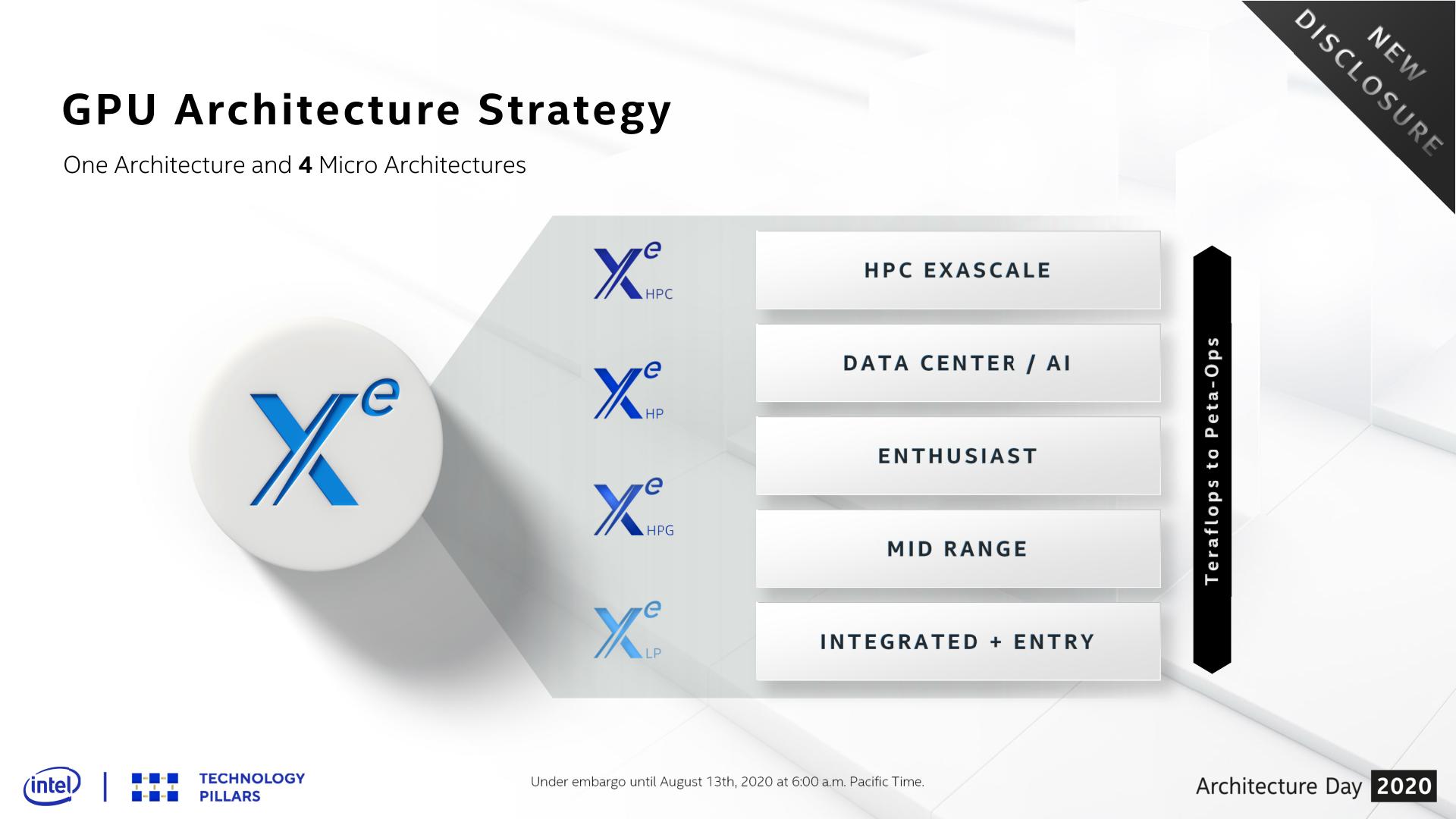
Since then, Intel has revised that plan a bit, and what was three microarchitectures is now four. Being announced as part of Intel Architecture Day today, Intel is revealing Xe-HPG, an additional microarchitecture for gaming-focused chips. We have more on Xe-HPG in this article, but at a high level it’s meant to be the missing piece of the puzzle in Intel’s product stack, offering a high-performance gaming and graphics-focused chip as opposed to Xe-HP, which is specializing in datacenter features like FP64 and multi-tile scalability. Xe-HPG is set to arrive in 2021, and notably will be built entirely at a third-party fab, unlike the rest of the Xe family.
Which to bring things back to the immediate topic of Xe-LP, makes this year’s launch of Intel’s first Xe microarchitecture all the more important. Intel’s plans for Xe involve building up successive Xe parts – quite literally in Xe-HPC’s case – going for wider designs that incorporate ever increasing numbers of base building blocks, and then scaling out the number of GPUs when even that isn’t enough. So Xe-LP is very much the foundation of the Xe family, not just in diagrams but in architecture as well; and consequently, what Intel has designed for Xe-LP will have repercussions for the entire Xe product stack.
Xe-LP: Integrated with Tiger Lake, But Discrete as Well
While Intel’s product plans for Xe have them eventually reaching far and wide, it’s only fitting that things start at the same place they always have for Intel’s GPUs: integrated graphics. Xe and Xe-LP will be making their first appearance in the market as part of Intel’s new Tiger Lake SoC, which the company will be launching on September 2nd. And despite the fact that Intel isn’t talking much about the product side of Tiger Lake itself – preferring to keep today about architecture and making September about products – Tiger Lake was very clearly the focal point for Xe-LP’s design. So Tiger Lake is the catalyst for it all, as we’ll see when discussing Xe-LP’s features.
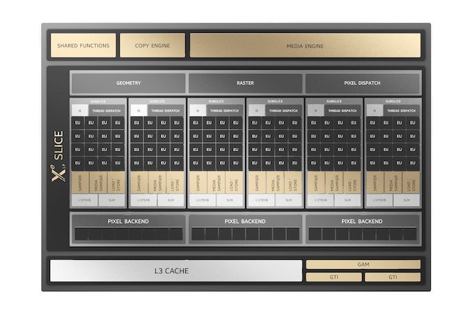
Given Intel’s official disclosures today (never mind the many, many leaks), it’s clear that Tiger Lake parts are going to top out with a single Xe-LP slice. Which, new with this generation, is now 96 of Intel’s more fundamental GPU Execution Units (EUs). Overall, the company is targeting a 2x increase in performance over Ice Lake (Gen11) graphics,
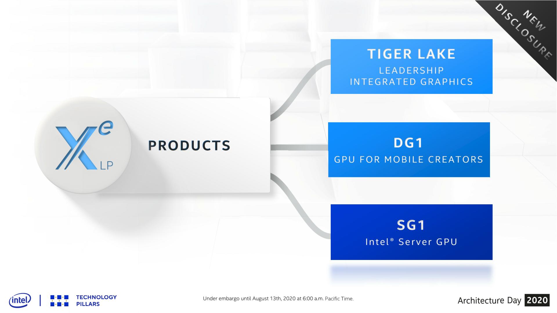
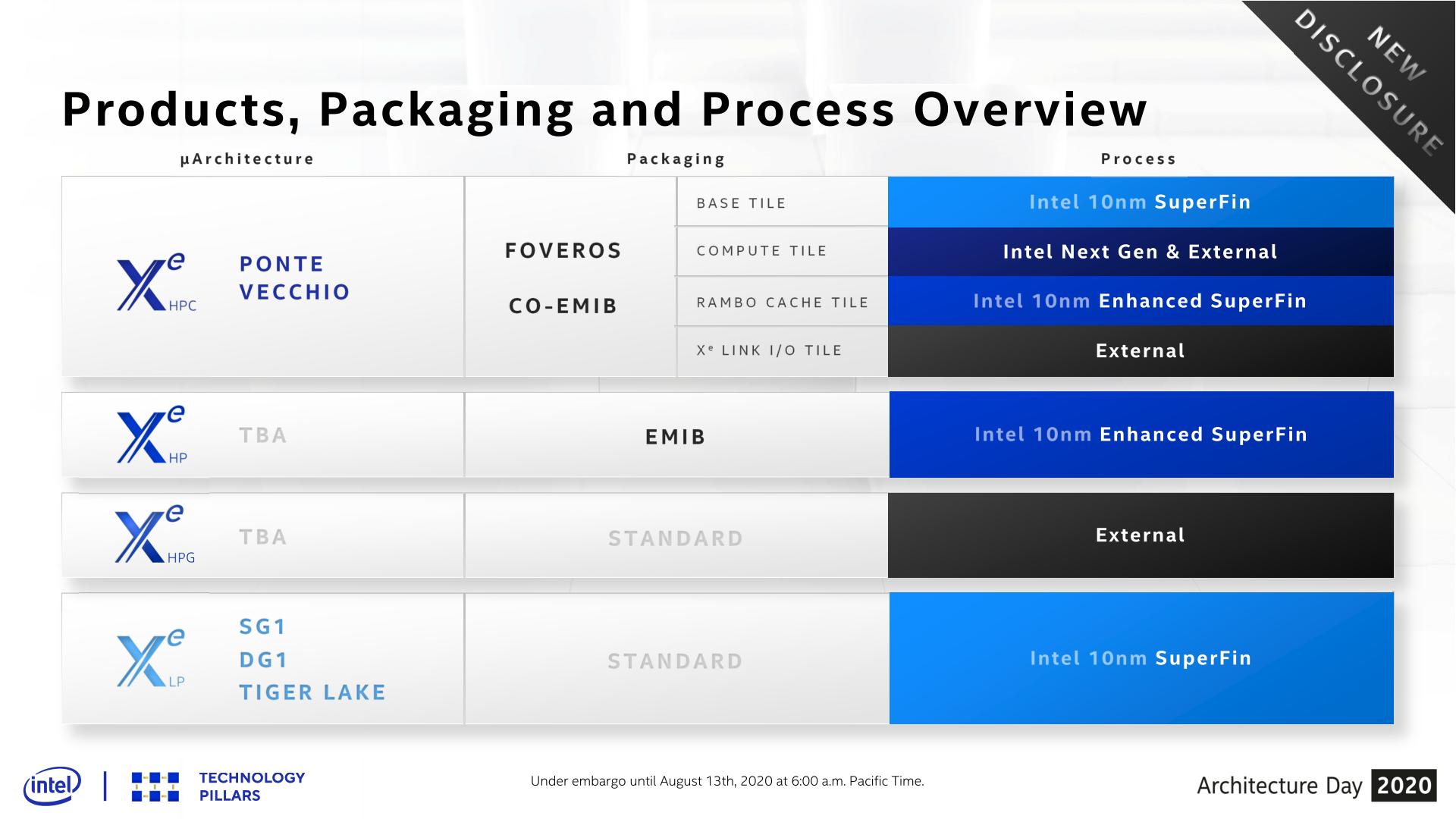
But Tiger Lake won’t be the only place where Xe-LP will show up. As previously disclosed by Intel, the company is developing a discrete GPU version of it, which they are calling DG1. Designed to be paired with Tiger Lake in notebooks and other mobile devices, DG1 is Intel’s first discrete GPU in over twenty years, and it’s the spiritual-successor of sorts to Intel’s GT3 and GT4e integrated GPU configurations. Only instead of building low-volume CPU designs with a larger GPU, Intel will instead sell OEMs a discrete GPU based on the same architecture and built on the same 10nm SuperFin process as the integrated GPU.
DG1 will be shipping this year, so expect to see it show up in higher-performing Tiger Lake laptops. However Intel is otherwise disclosing very little about the part, as they are not disclosing much of anything with regards to product configurations today. So while we know that it’s based on Xe-LP and that it’s mobile-focused (Intel has dropped all discussion of desktop usage), we don’t have official details on anything such as its configuration or what type of memory it uses.
And forming the final pillar, the sever space won’t be left out on Xe-LP either. Intel will be delivering a quad-GPU product for servers that they are calling SG1. Based on four DG1 GPUs, this will be a replacement of sorts for Intel’s Xeon Visual Compute Accelerator family of products. Designed to leverage Intel’s earlier integrated GPUs, the Xeon VCA cards were aimed at the video encoding market, using Intel’s QuickSync media blocks to accelerate the process. Now that Intel has discrete GPUs, they no longer need to gang together CPUs for this market, and instead can sell accelerators with just the GPU. It’s a bit of a niche market with regards to the larger GPU ecosystem, but it’s an important one for Intel, so they’re hoping that SG1 will make server operators stand up and take notice – or at least those pesky Goa'ulds.


33 Comments
View All Comments
Cooe - Saturday, August 15, 2020 - link
Soooooo much die space & transistors needed for just barely better performance than Renoir's absolutely freaking MINISCULE Vega 8 iGPU block.... Consider me seriously unimpressed. The suuuuuper early DDR5 support on the IMC is incredibly intriguing and I'm really curious to see what the performance gains from that will be like, but other than that.... epic yawn. Wake me up when it doesn't take Intel half the damn die for them to compete with absolutely teeny-tiny implementations of AMD's 2-3 year old GPU tech....Makes sense now why AMD's going for Vega again for Cézanne. Some extra frequency & arch tweaks are all they'd need to one-up Intel again, & going RDNA/2 would have had a SIGNIFICANTLY larger die space requirement (an RDNA dCU ["Dual Compute Unit"] is much, MUCH larger than 2x Vega II /"Enhanced" CU's), that just doesn't really make much sense to make until DDR5 shows up with Zen 4 and such a change can be properly taken advantage of.
(Current iGPU's are ALREADY ridiculously memory bandwidth bottlenecked. A beefy RDNA 2 iGPU block would bring even 3200MHz DDR4 to its absolute KNEES, & LPDDR4X is just too uncommon/expensive to bank on it being used widely enough for the huge die space cost vs iterating Vega again to make sense. Also, as we saw with Renoir; with some additional TLC, Vega has had a LOT more left in the tank than probably anyone of us would have thought).
Oxford Guy - Tuesday, August 18, 2020 - link
MadTV is back, with an episode called Anandtech Literally?Oxford Guy - Tuesday, August 18, 2020 - link
"t’s worth noting that this change is fairly similar to what AMD did last year with its RDNA (1) architecture, eliminating the multi-cycle execution of a wavefront by increasing their SIMD size and returning their wavefront size. In AMD’s case this was done to help keep their SIMD slots occupied more often and reduce instruction latency, and I wouldn’t be surprised if it’s a similar story for Intel."Retuning or returning to?