Qualcomm Announces New Snapdragon Wear 4100 & 4100+: 12nm A53 Smartwatches
by Andrei Frumusanu on June 30, 2020 11:00 AM EST- Posted in
- Wearables
- Qualcomm
- Snapdragon Wear
- Snapdragon Wear 4100
Today Qualcomm is making a big step forward in its smartwatch SoC offerings by introducing the brand-new Snapdragon Wear 4100 and Wear 4100+ platforms. The new chips succeed the aging two 2018 originating Wear 3100 platforms and significantly upgrading the hardware specifications, bringing to the table all new IPs for CPU, GPU and DSPs, all manufactured on a newer lower power process node.
Smartwatch products over the last few years had always one big criticism to them, and that was the fact that the SoCs powering them were always seemingly underpowered compared to what we’re seeing from the like of vertically integrated vendors such as Apple and their own smartwatch SoCs. Qualcomm’s new Wear 4100 SoC now finally abandons the Cortex-A7 cores and 28nm process in favour of Cortex-A53 cores and a 12nm process – whilst certainly not bleeding edge, it’s a big jump in performance and power efficiency.
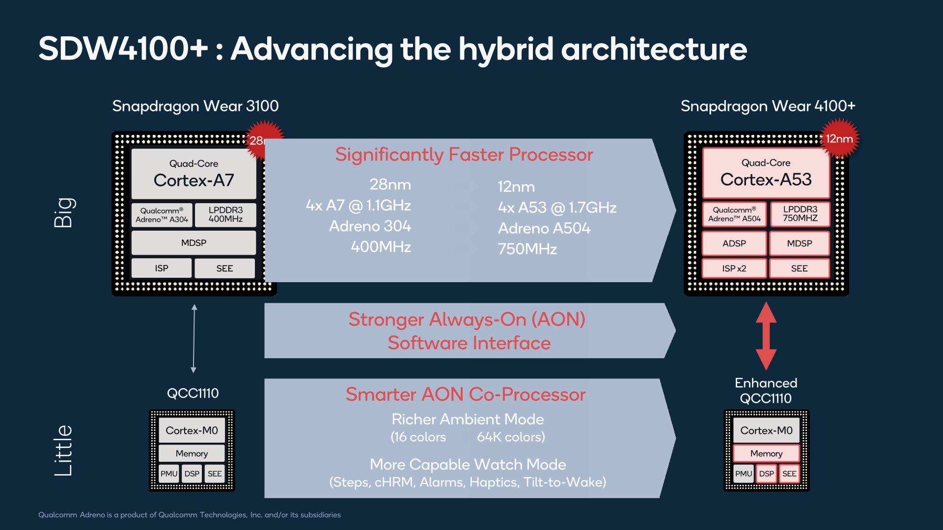
The new SoC is a complete overhaul in terms of design. As mentioned, instead of the quad-core A7 cores at 1.1GHz, the new chip now features quad A53 cores at up to 1.7GHz. The chip still relies on LPDDR3 as its memory technology but the clock rates have been upped from 400MHz to 750Mhz. The GPU has seen a giant leap in performance as it sees the jump of 2 architectural generations from an Adreno 304 to a new Adreno 504. The chipset also seen its DSP capabilities expanded as it now features a second dedicated audio DSP for actual application side processing (Alongside the modem DSP) that previously didn’t exist on the Wear 3100 chip.
An interesting addition to the SoC is a second ISP. The new chip is able to now handle dual 16MP cameras – some of Qualcomm’s customers have ideas for smartwatch products which would deploy two cameras.
The main SoC is now manufactured on a newer 12nm process node at TSMC – it’s certainly not the newest node given a new platform like this, but Qualcomm probably made their cost-performance calculations when choosing this design aspect.
It's to be noted that it looks like Qualcomm did recycle the design from the Snapdragon 429 - although it's possible the Wear variant here might be specifically binned for low power usage.
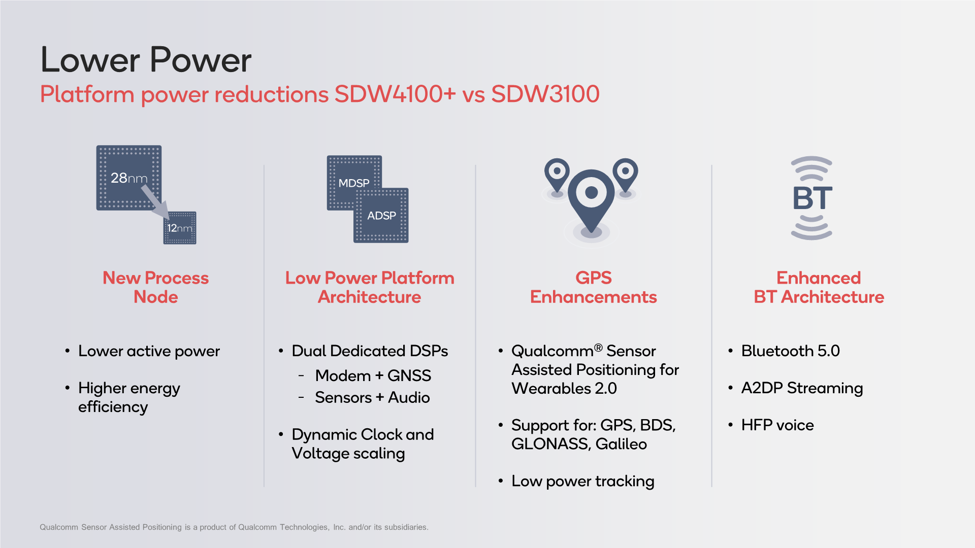
Connectivity wise, the chip still employs a LTE category 4 modem with up to 150Mbps down and 50Mbps up speeds, but the new RF system includes optimisations for power usage, such as the new addition of eDRX (Extended discontinuous reception) for much better power efficiency. Bluetooth connectivity has been upgraded to the 5.0 standard.
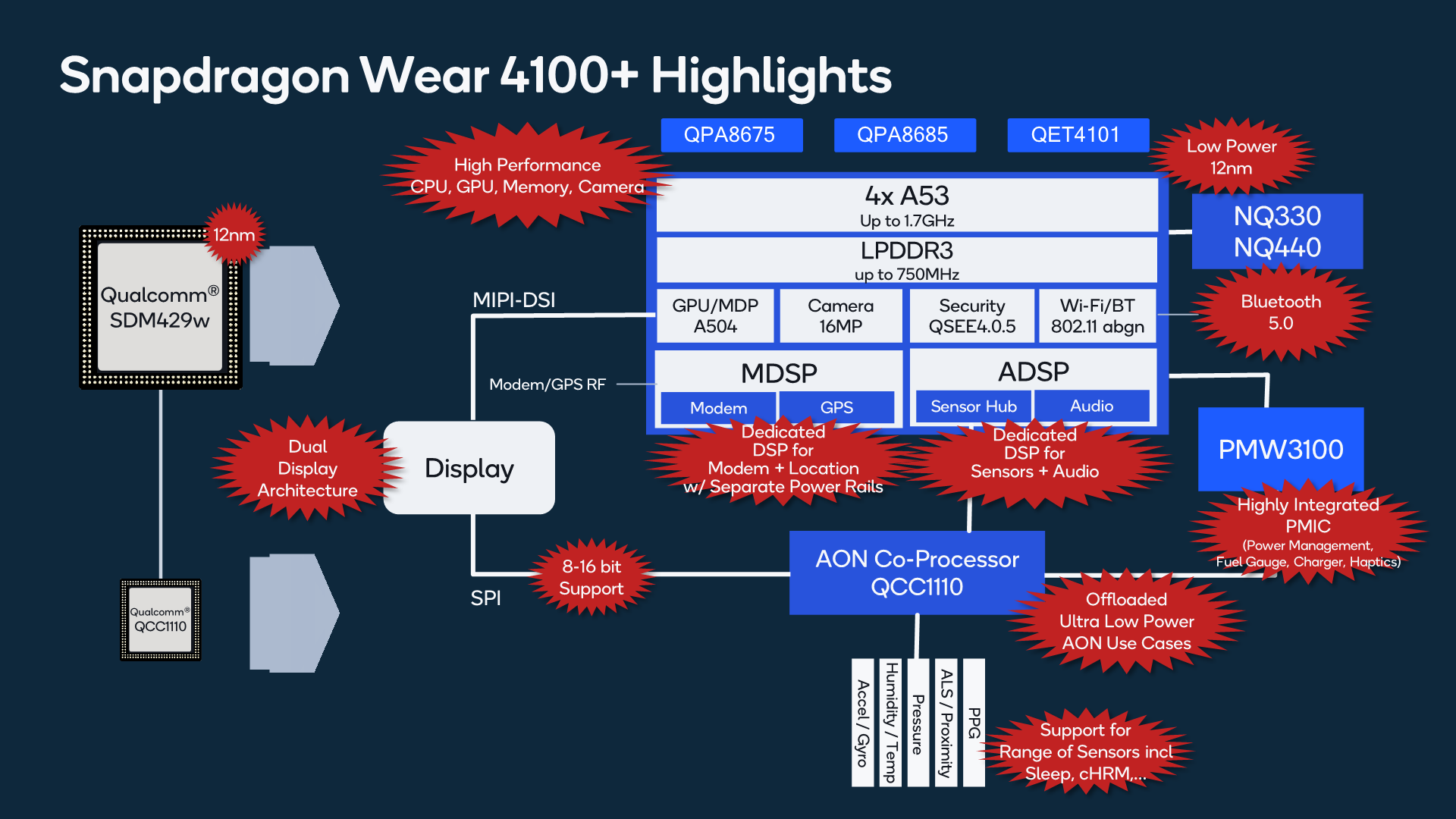
Qualcomm continues to use a main SoC + co-processor architecture for its smartwatch platforms. The aforementioned Wear 4100 serves as the main processor chip during active and interactive usage of the device, whilst a secondary co-processor serves as the always-on silicon that is able to enable ambient non-interactive device use-cases (Essentially, powering on the screen with static / low-updating information).
The co-processor has a similar design to the QCC1110 that was bundled with the Wear 3100 platform, but has been enhanced in terms of some of its capabilities such as having richer colour depth rendering ability for up to 16 bit (64K colours).
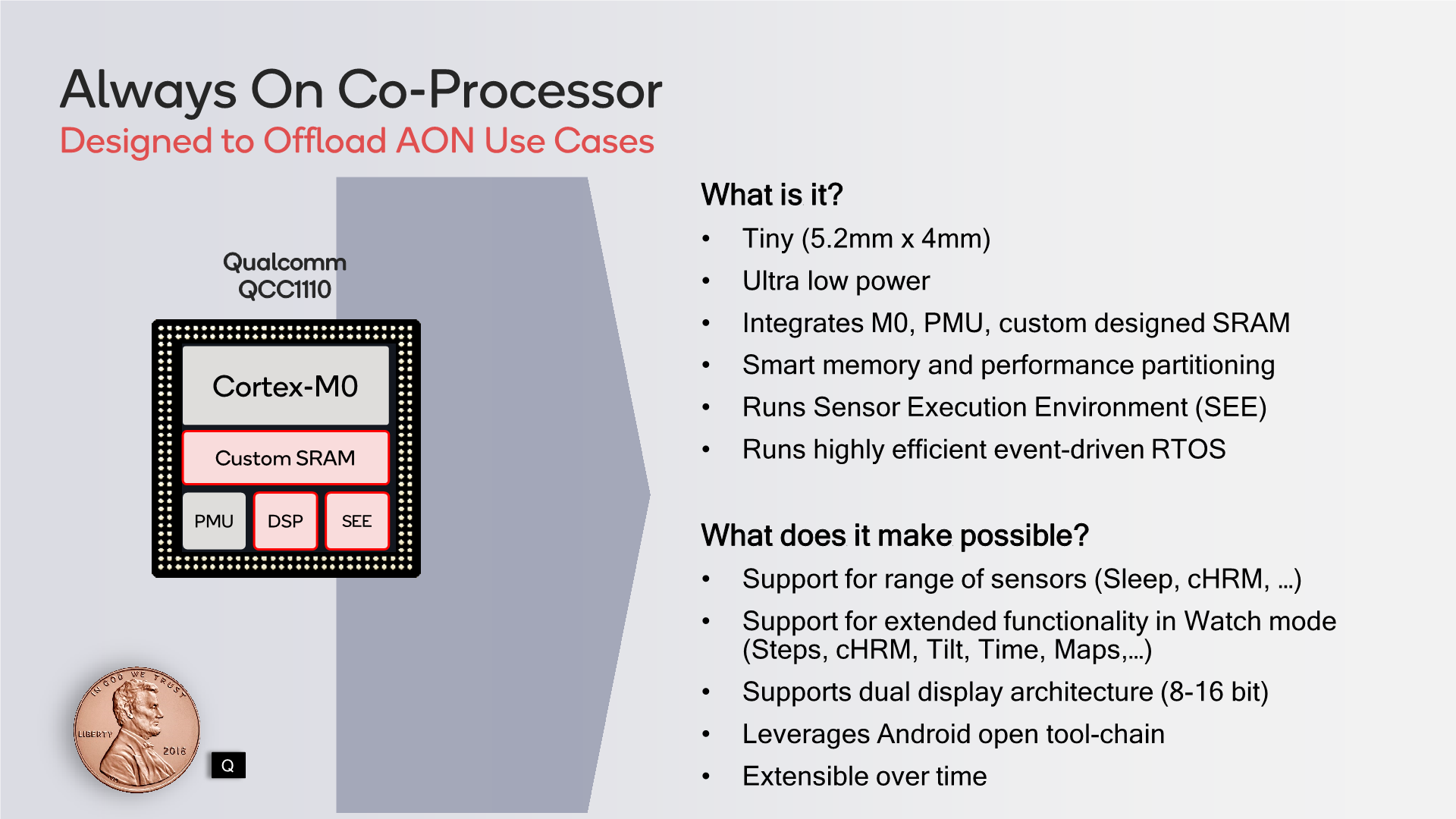
The key aspect for using both a main SoC and a co-processor in the same device is the dual display architecture of the system, where the display is connected to both chip and can receive signals from both. The reason for Qualcomm to not have implemented a single monolithic chip is rationalised by design efforts and cost-opportunity; while they haven’t announced any products yet, they envision the possibility to use the QCC1110 as a standalone system in a device, and likewise, one can use the Wear 4100 without a co-processor.
The co-processor can serve as the sensor hub collecting data from your typical smartwatch sensors, all whilst the main SoC is powered off.
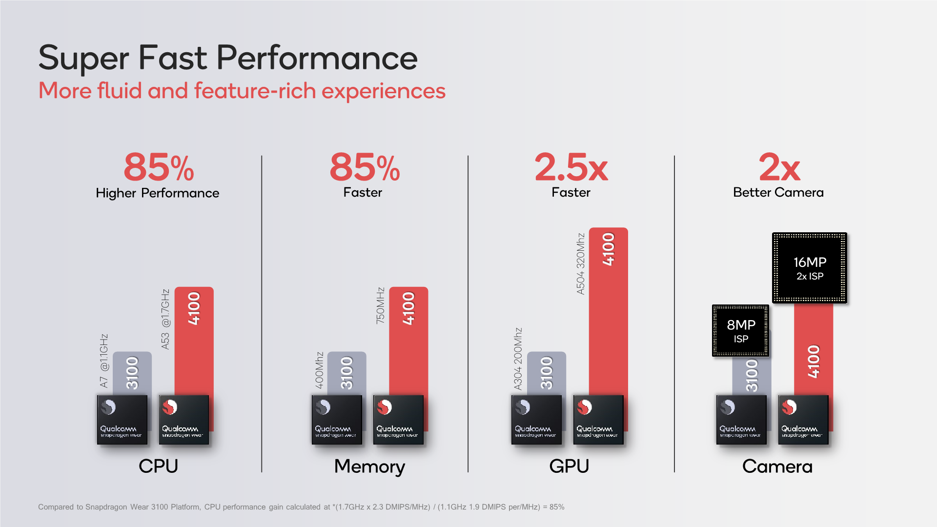
The overall improvements of the platforms bring a -20% decrease in power usage, all whilst increasing CPU performance by 85%, GPU performance by a massive factor of 2.5x. In terms of workload efficiency, you’ll be seeing significant increases – all needed in wearable devices as battery life is key.
The Snapdragon Wear 4100 platform represents the main SoC and surrounding essential components, whilst the Wear 4100+ platform also includes the co-processor for augmented always-on operation. The new platforms are available and shipping to vendors now.
Related Reading:
- Qualcomm Launches Snapdragon Wear 3100 Platform for Smartwatches
- Qualcomm Announces Snapdragon Wear 2100 IoT SoC
- Qualcomm Announces Snapdragon Wear 1200 SoC: LTE Categories M1 & NB1 for Wearables & Smart Trackers
- Qualcomm Announces Snapdragon Wear 1100 SoC For Wearables
- Apple Announces The Apple Watch 4: Fully Custom SiP


33 Comments
View All Comments
dotjaz - Friday, July 10, 2020 - link
Also TSMC disagrees with you by developing 22ULP and 12FFC+ULL, 22ULP only entered mass production in 2019 or later considering risk production was Q4 2018.22ULP from TSMC, 22FFL from Intel, 22FDX-ULL from GloFo are the leading ultra low power solutions, notice the trend?
https://www.tsmc.com/english/dedicatedFoundry/tech...
https://www.tsmc.com/english/dedicatedFoundry/tech...
dotjaz - Friday, July 10, 2020 - link
Forgot about Samsung, their version is 28FDS/18FDS and 8LPU as ultra low power solution. Again, nothing below 10nm (8LPU is still 10nm)RSAUser - Saturday, July 11, 2020 - link
You're linking for ultra low power, smart watches do not fall into that category yet as ULL is probably still a little too weak.You'd use ULP in IoT for things like a sensor for room temperature, etc. where it's never something that needs to be able to complete something quickly, like responding as fast as possible to a user's touch input on a watch and driving a graphical display that's constantly changing.
CaptainElwood - Tuesday, June 30, 2020 - link
This is such great news! I cannot stand iOS but am so reliant on my Apple watch I can't switch back to Android. I tried out a gen 5 fossil watch and it is really close to being sufficient, and I actually get about the same battery life as my apple watch 4 LTE (fossil doesn't have cell service). This update, while mediocre, will at least be enough to use wearOS.Makaveli - Tuesday, June 30, 2020 - link
Has hell frozen over they finally updated the SOC on these!name99 - Tuesday, June 30, 2020 - link
"some of Qualcomm’s customers have ideas for smartwatch products which would deploy two cameras"Smartwatch products? Or IoT products that would use this SoC?
I still don't see how camera on a Smartwatch makes sense. It's really difficult to twist your wrist into a useful angle for almost any use case you can imagine. Certainly not taking normal photos, but even QR codes is tough, and while you can imagine a video call, try it and you'll see that
- your wrist/arm hurts like hell after ten seconds or so
- the image shakes like crazy
Watch on cameraI just don't see.
But companies like Arlo or Wyze using a Watch SoC for their cameras. Or a company like Ecobee using a mini camera in the thermostat and even the sensor units (to track who is in which room, for finer gradations of temperature management), that I could see.
iampivot - Wednesday, July 1, 2020 - link
The dual camera support is probably for use with google glass type devices.name99 - Wednesday, July 1, 2020 - link
Good analysis! Yeah, that makes sense.trivik12 - Tuesday, June 30, 2020 - link
I am curious as to what chipset Samsung will use for GW3. I hope that is A55 based and lowest possible leakage process.shabby - Wednesday, July 1, 2020 - link
Is qualcomm comparing a 2012 soc to a 2011 soc in their graphs? lol