Intel: Tiger Lake Client CPUs Coming Mid-Year
by Ryan Smith on April 24, 2020 10:00 AM EST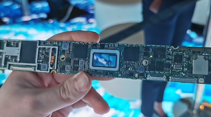
Along with detailing the nuts and the bolts of their Q1 2020 earnings, as part of Intel’s financial presentation, the company also offered a quick update on their upcoming Tiger Lake client CPUs. In short, the company is now preparing for volume production of the chips, and expects to being shipping them to OEMs mid-year.
Intel first unveiled Tiger Lake back at CES 2020 early this year, where the company briefly detailed the architecture while showing off a device using a prototype chip. Tiger Lake will be based on Intel’s latest Core CPU architecture, and will also be the first CPU from the company to integrate an iGPU based on their new Xe-LP graphics architecture. The chips will be based on a newer version of Intel’s 10nm manufacturing process than what’s used in the current ice Lake chips, which Intel is calling their 10+ process. At the time, Intel was promising that Tiger Lake devices would show up by the holidays, a similar time frame as 2019’s Ice Lake launch.
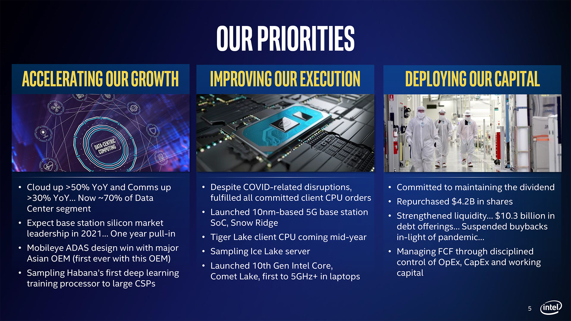
All told then, Intel’s most recent update is right in-line with their previous promises. With Tiger Lake being another mobile-first launch, OEMs need to receive chips well in advance of when consumer products will reach the store shelves, both to give OEMs the necessary time to finalize their designs, as well as to build up a suitable stockpile of devices for a proper retail launch. So, as it always needs to be said when talking about Intel’s timelines for manufacturing, while Tiger Lake chips will be shipping mid-year, we’re not currently expecting devices any sooner than what Intel has previously discussed.
Finally, if everything goes according to plan or Intel, it looks like the Tiger Lake launch should be a higher volume affair than Ice Lake’s. Cognizant of Ice Lake’s slow ramp-up and launch in 2019, Intel is telling investors that they are holding twice as many Tiger Lake CPUs in reserve as compared to Ice Lake. The company does need to master its updated 10+ process to get there, but with any luck, Intel’s 4+ years of playing with 10nm may finally pay some better dividends as they bring up their latest process.
#ontherun #TigerLake pic.twitter.com/Dhm1TwlcjV
— 𝐷𝑟. 𝐼𝑎𝑛 𝐶𝑢𝑡𝑟𝑒𝑠𝑠 (@IanCutress) January 8, 2020


140 Comments
View All Comments
Oxford Guy - Sunday, April 26, 2020 - link
"My sense is that each new manufacturing node is significantly more expensive than the last."A TSMC person, a few years ago, stated how many design rules needed to be used for the different nodes. The number of design rules (complexity of design) increased very rapidly with node shrinkage.
Deicidium369 - Saturday, April 25, 2020 - link
Dividends are not vital but are expected - they do not horde cash overseas like ApplePriorities are to the invenstors / shareholders
Pretty sure paying dividends are not the reason that Ice Lake was released when it was - was released when it was ready
Oxford Guy - Saturday, April 25, 2020 - link
It's about time for Anandtech to post a detailed article about the actual node sizes involved in all of the different CPUs on the market and coming soon.The fake nm naming stuff is intentionally confusing for consumers. It's not good enough to just relegate the truth to some random comments in articles.
Wilco1 - Saturday, April 25, 2020 - link
What really matters is the actual transistor density of real devices. As opposed to marketing.TSMC 7nm: 90.9 million transistors / mm^2 (Kirin 990 5G)
Intel 10nm: 49.4 MT/mm^2 (Lakefield compute die)
So that shows for mobile SoCs, Intel 10nm is nowhere near TSMC in real density.
https://en.wikipedia.org/wiki/Transistor_count
https://fuse.wikichip.org/news/3417/a-look-at-inte...
yeeeeman - Saturday, April 25, 2020 - link
Efficiency for the Intel node is also much worse than tsmc 7nm.yeeeeman - Saturday, April 25, 2020 - link
Basically the revised 10nm node is just a bit denser than 14nm. Much much different than what they intended in the first place where they stated 100mtr/ mm2, better than tsmc 7nm.Deicidium369 - Saturday, April 25, 2020 - link
in what way? power usage? Power usage is quite efficient on Ice Lake and assuming Tiger Lake.and, no 10nm+ is not a bit denser than 14nm - 10+ reaches the initial target of 2.7x density increase.
Intel traditionally has multiple architectures - some frequency optimized (current 5GHz+) or power optimized (lakefield, Ice Lake) or density optimized. The 10nm is focused on power efficiency, 10nm+ will focus on density and (Ice Lake Servers) and frequency is likely never to reach 14nm levels - but then again neither can any node from TSMC
AMD's Zen 2 compute complex is 30-36M/mm^2 Intel 14nm is 37-45M/mm^2. Source - https://www.reddit.com/r/Amd/comments/ecca4s/trans...
Spunjji - Monday, April 27, 2020 - link
Your AMD numbers are wrong. Zen 2's *compute complex* is 52.7MTr/mm^2. You quoted the density of the *entire chip*, which includes the 14nm IO die. Renoir - which is entirely 7nm - is up at 63.33MTr/mm^2.https://www.reddit.com/r/Amd/comments/fraqll/amd_s...
As for your claims about Intel's 10nm+ density, I literally can't find any solid information that would confirm or refute it. You're effectively quoting their original 10nm marketing slides verbatim and expecting that to hold up in reality.
name99 - Monday, April 27, 2020 - link
Intel's best case real world scenario 10nm density numbers are for Lakefield's compute die. This die omits all those large IO transistors, and has no requirements to be blazing fast. Even so, yeah, half the density of TSMC...You can find the raw numbers here if you want to do your own calculation:
https://fuse.wikichip.org/news/3417/a-look-at-inte...
Spunjji - Tuesday, April 28, 2020 - link
Cheers for the sauce. I'm amazed they missed their advertised numbers by that far, especially given the relatively small caches and offloaded IO. Given the purported numbers for Ice Lake, though, I do wonder if there's something missing from the story here.Foveros looks quite promising as a future technology. Right now, though, it's amusing they had to do all of that just to reach comparable board space requirements (but not power/performance parity) with Apple's ARM designs.