Samsung Develops Smaller DDR4 Dies Using 3rd Gen 10nm-Class Process Tech
by Anton Shilov on March 21, 2019 11:30 AM EST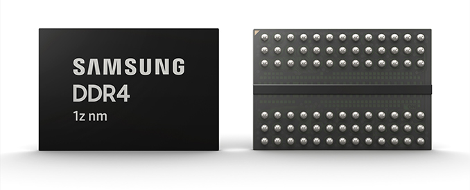
Samsung has completed development of its 3rd-generation 10 nm-class manufacturing process for DRAM as well as the first 8 Gb DDR4 chip that uses the technology. The 1z-nm process technology is said to be the world’s smallest process node for memory, and will enable Samsung to increase productivity without needing to go to extreme ultraviolet lithography (EUVL) at this time. The company plans to start volume production using the technology in the second half of 2019.
Samsung says that its 3rd Generation 10 nm-class manufacturing technology (also known as 1z-nm) for DRAM enables it to make 20% more 8 Gb DDR4 memory chips per wafer than the 2nd Gen 10-nm class (aka 1y-nm) does. An increase of the number of dies per wafer essentially means that the new 8 Gb DDR4 device is approximately 20% smaller* than the previous-gen 8 Gb DRAM, which means a tangible decrease of production costs at the same yield and at the same cycle time. This should mean cheaper DRAM pricies for consumers.
Samsung traditionally does not disclose exact smallest half-pitch size of the new memory device, so at this time we do not have any information about the new chip’s geometries. Since we are dealing with a 1z node, it is reasonable to assume that the smallest half-pitch size is well below 15 nm, but this is speculation.
The world’s largest maker of memory is especially proud that its 3rd Generation 10 nm-class manufacturing technology for DRAM continues to use ArF (argon fluoride) immersion lithography tools and does not require EUVL. Keeping in mind that ultra-thin nodes require multi-patterning in case of immersion lithography, it is logical to assume that Samsung uses this method along with various tricks to ensure good yields and performance.
Samsung will start production of 8 Gb DDR4 memory chips using its 1z-nm fabrication process in the second half of the year. The first products based on the 8 Gb 1z chips will be DDR4 DRAM modules. Once they are validated by CPU designers, they will be used for PCs in 2020.
Going forward, the same manufacturing technology will be used to produce DRAMs with “higher capacities and performance”.
Related Reading
- Samsung Starts Production of 8 Gb DDR4-3600 ICs Using 2nd Gen 10nm-Class Tech
- Samsung Begins To Produce DDR4 Memory Using '10nm Class' Process Tech
- Samsung Demos 64 GB RDIMM Based on 16 Gb Chips, Promises 256 GB LRDIMMs
Source: Samsung
*Note: This is a very rough calculation.


28 Comments
View All Comments
Notmyusualid - Friday, March 22, 2019 - link
So are we going to get modules with better CL levels, or is this just for THEIR benefit?rpg1966 - Friday, March 22, 2019 - link
Yes, damn these charities not giving away free memory.You realise they need to make profits to justify the investment, right? You realise that prices go up and down, and they need to make hay while the sun shines? You realise that if they don't make reasonable profits, you don't get the tech you desire? You realise... no, you probably don't.
Irata - Friday, March 22, 2019 - link
If you look at earnings before taxes in many industries (does not matter if it's tech, finance, energy), then "reasonable" is not the word that comes to mind.Not saying that companies do not need to make a profit on the goods and services they provide - that's the reason they are doing what they are doing - oh, and of course to make the world a better place for everyone - I almost forgot that.
But there is a point when "reasonable" no longer applies and once it does, this is also the point when it is at the consumers' expense as profits are higher than they should be in an ideal free market economy.
close - Friday, March 22, 2019 - link
Really funny how Samsung plays around with the "10nm class" technology."Samsung says that its 3rd Generation 10 nm-class manufacturing technology (also known as 1z-nm) for DRAM enables it to make 20% more 8 Gb DDR4 memory chips per wafer than the 2nd Gen 10-nm class (aka 1y-nm) does"
1z, 1y, 1*. Basically saying that number replaced by a letter is anything but a 0. They were probably 19nm for 1y and 15-16nm for 1z.
I'll just throw this next to my 10Yottabyte-class SSD (0.00000000000001 Yottabytes for anyone who's asking). Still Yottabyte-class I guess since I managed to use it in the same sentence while being mathematically correct.
frenchy_2001 - Monday, March 25, 2019 - link
First generation is X actually (so 1X), followed by 1Y then 1Z.You are probably right theat 1X was close to 20 (so probably 19 or 18). 1Y in mid 10s and now 1Z in low 10s.
Giving generations like that avoid the marketing names foundries have been using for logic chips.
Ex: 16nm, 12 nm (which is really only an optimized 16nm), 10nm... and so on.
There is very little relation nowadays between the node name and its critical dimensions.
BenJeremy - Friday, March 22, 2019 - link
Am I the only one that remembers the glorious Samsung 4GB Magic RAM sticks from years ago?Remember when $20 for 4GB was a low price in 2012? Glad RAM is so much cheaper these days... wait, what?
Dolda2000 - Friday, March 22, 2019 - link
Any info on what these higher densities mean for things like row hammer attacks?ianmills - Thursday, March 28, 2019 - link
Being an OLED and presumably pentile screen, does this not mean the effective resolution is 1080x(2/3)= 720p? Seems like such a waste to have effective 720p screen on such a big phone. No matter much the price it is not a good tradeoff IMHO