Samsung Starts Mass Production of Chips Using Its 7nm EUV Process Tech
by Billy Tallis & Anton Shilov on October 17, 2018 6:00 PM EST- Posted in
- Semiconductors
- Samsung
- EUV
- 7nm
- Samsung Foundry
- 7LPP
Samsung Foundry on Wednesday said that it had started production of chips using its 7LPP manufacturing technology that uses extreme ultraviolet lithography (EUVL) for select layers. The new fabrication process will enable Samsung to significantly increase transistor density of chips while optimizing their power consumption. Furthermore, usage of EUVL allows Samsung to reduce the number of masks it requires for each chip and shrink its production cycle.
New Tech Brings in Big Gains
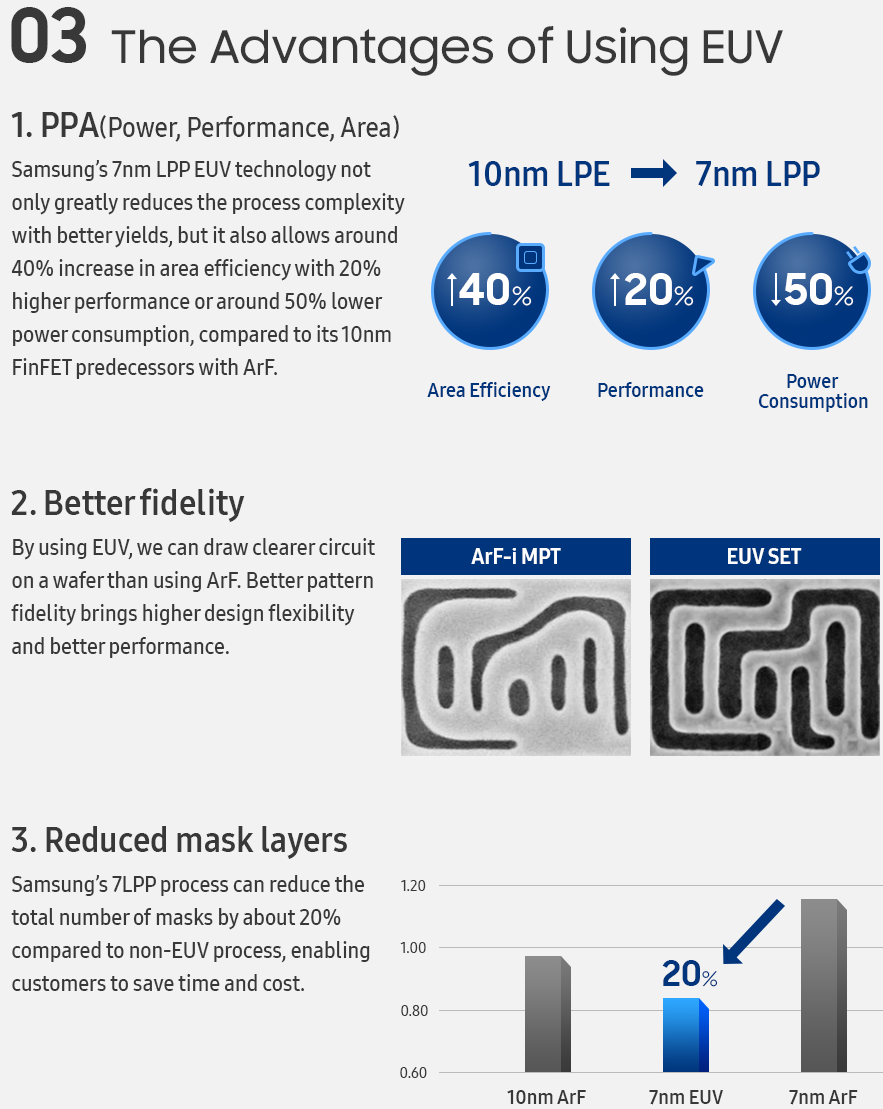
The maker of semiconductors says that 7LPP fabrication technology enables a 40% area reduction (at the same complexity) along with a 50% lower power consumption (at the same frequency and complexity) or a 20% higher performance (at the same power and complexity) when compared to 10LPE. As it appears, usage of extreme ultraviolet lithography for select layers enables Samsung Foundry to place more transistors inside its next-gen SoCs and reduce their power consumption, a very compelling proposition for mobile SoCs that will be used inside future flagship smartphones.
| Advertised PPA Improvements of New Process Technologies Data announced by companies during conference calls, press briefings and in press releases |
||||||||
| 14LPP vs 28LPP |
10LPE vs 14LPE |
10LPE vs 14LPP |
10LPP vs 10LPE |
10LPU vs 10LPE |
7LPP vs 10LPE |
|||
| Power | 60% | 40% | 30% | ~15% | ? | 50% | ||
| Performance | 40% | 27% | >10% | ~10% | ? | 20% | ||
| Area Reduction | 50% | 30% | 30% | none | ? | 40% | ||
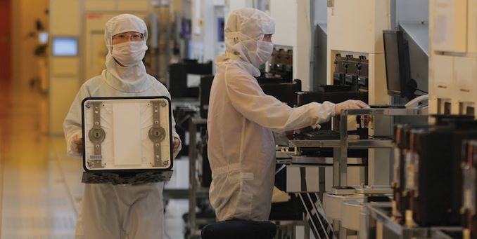
Samsung produces its 7LPP EUV chips at its Fab S3 in Hwaseong, South Korea. The company can process 1500 wafers a day on each of its ASML Twinscan NXE:3400B EUVL step and scan systems with a 280 W light source. Samsung does not say whether it uses pellicles that protect photomasks from degradation, but only indicates that usage of EUV enables it to cut the number of masks it requires for a chip by 20%. In addition, the company says that it had developed a proprietary EUV mask inspection tool to perform early defect detection and eliminate flaws early in the manufacturing cycle (which will likely have a positive effect on yields).

Samsung Foundry does not disclose the name of its customers that that first to adopt its 7LPP manufacturing technology, but only implies that the first chips to use it will be aimed at mobile and HPC applications. Usually, Samsung Electronics is the first customer of the semiconductor unit to adopt its leading-edge fabrication processes. Therefore, expect a 7nm SoC inside Samsung’s high-end smartphones due in 2019. Furthermore, Qualcomm will use Samsung’s 7LPP tech for its “Snapdragon 5G mobile chipsets”.
“With the introduction of its EUV process node, Samsung has led a quiet revolution in the semiconductor industry,” — said Charlie Bae, executive vice president of foundry sales and marketing team at Samsung Electronics. “This fundamental shift in how wafers are manufactured gives our customers the opportunity to significantly improve their products’ time to market with superior throughput, reduced layers, and better yields. We’re confident that 7LPP will be an optimal choice not only for mobile and HPC, but also for a wide range of cutting-edge applications.”
Advanced IP and Packaging: Ready for 7LPP
Samsung’s 7LPP manufacturing technology offers impressive advantages over the company’s 10LPE specifically for mobile SoCs. Meanwhile, in a bid to make the process attractive to a broad range of potential customers, the foundry offers a comprehensive set of design-enablement tools, interface IP (controllers and PHY), reference flows, and advanced packaging solutions. The final PDK is months away, but many customers may start development of their 7LPP SoCs even with existing set of solutions.
At this point 7LPP is supported by numerous Samsung Advanced Foundry Ecosystem (SAFE) partners, including Ansys, Arm, Cadence, Mentor, SEMCO, Synopsys, and VeriSilicon. Among other things, Samsung and the said companies offer such interface IP solutions HBM2/2E, GDDR6, DDR5, USB 3.1, PCIe 5.0, and 112G SerDes. Therefore, developers of chips of SoCs due in 2021 and onwards, which will rely on PCIe Gen 5 and DDR5, can start designing their chips right now.
As for packaging, chips made using 7LPP EUV technology can be coupled with 2.5D silicon interposer (if HBM2/2E memory is used) as well as Samsung’s embedded passive substrates.
Expanding EUV Capacity
As noted above, Samsung installed EUV production tools at its Fab S3, which still has plenty of DUV (deep ultraviolet) equipment. As EUVL is used only for select layers of 7LPP chips, the relatively limited number of Twinscan NXE:3400B scanners is hardly a problem, but when Samsung’s process technologies will require EUV for more layers, it may need to expand its EUV capacities.
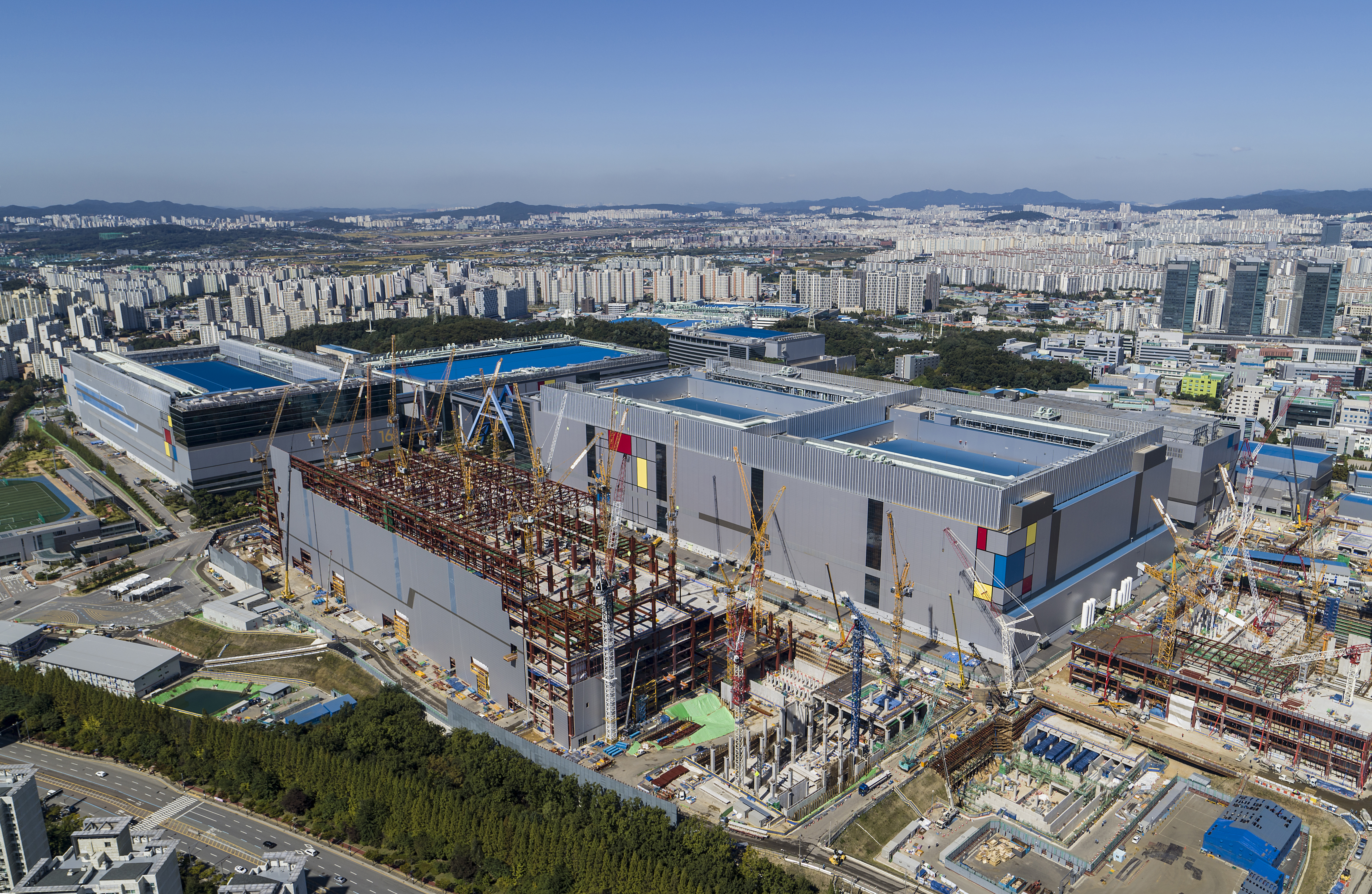
As reported in September, a major increase of EUV lithography usage by Samsung Foundry will happen after it builds another production line in Hwaseong, which was architected for the EUV tools from the start. The fab is set to cost 6 trillion Korean Won ($4.615 billion), it is expected to be completed in 2019, and start HVM in 2020.
33 Years in Development
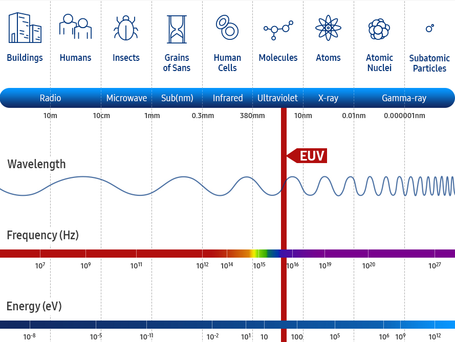
The launch of commercial production of chips using extreme ultraviolet lithography is a culmination of work by the whole semiconductor industry that began in 1985. Ultimately, EUVL is expected to reduce usage of multi-patterning when producing complex elements of a chip and therefore simplify design process, improve yields, and shrink cycle times (or rather not make them longer in the foreseeable future).
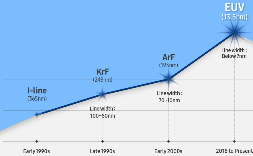
Meanwhile, it was extremely challenging to bring EUV from drawing boards to actual fabs because the technology is extremely complex. It needs all-new step-and-scan systems outfitted with all-new light source, new chemicals, new mask infrastructure, and numerous other components that took years to develop. To learn more about EUV lithography, please check our article from 2016.
Related Reading:
- EUV Lithography Makes Good Progress, Still Not Ready for Prime Time
- Samsung Foundry Updates: 8LPU Added, EUVL on Track for HVM in 2019
- Arm and Samsung Extend Artisan POP IP Collaboration to 7LPP and 5LPE Nodes
- Samsung Foundry Updates: 8LPU Added, EUVL on Track for HVM in 2019
- Samsung Foundry Roadmap: EUV-Based 7LPP for 2018, 3 nm Incoming
- Arm and Samsung Extend Artisan POP IP Collaboration to 7LPP and 5LPE Nodes
- Samsung’s 8LPP Process Technology Qualified, Ready for Production
- Samsung and TSMC Roadmaps: 8 and 6 nm Added, Looking at 22ULP and 12FFC
- TSMC Details 5 nm Process Tech: Aggressive Scaling, But Thin Power and Performance Gains
- TSMC Kicks Off Volume Production of 7nm Chips


42 Comments
View All Comments
ZolaIII - Friday, October 19, 2018 - link
The cost of development & testing increased significantly and FinFET structures aren't suitable for analog or mixed components. & it's all about complexity number of steps and masks, patterns. That's why EUV is so important as it reduces number of nedded patterns lowering the number of steps & driving the cost down. In time evaluation period will also go down cutting the design cost. TSMC rushed their first gen 7nm FinFET using lo density lib & it has relatively small advantages over their last 10nm node especially regarding density. They won QC deal thanks to timing. Samsung is currently in lead regarding 7nm and it is "very suitable" as it's at least 30% cheaper per gate to non EUV 7nm and 66% denser than Samsungs own 10nm which is in both cases huge. On the other hand they don't have a timing on their side but they will have a lot of free capacity while TSMC is currently over crowded. GloFo disappointed dropping the 7nm node, while 22nm FD-SOI is good & cutting edge for analog and mixed, relatively cheap and good enough for main stream & lower tier mobile being the first choice for IoT it simply ain't good enough for HPC & beading edge mobile. If GloFo had both it would have become really interesting with unique win win mix of available node's & capabilities. Samsung does own the most IP's & has the largest offering of IP's and licensable IP's for it's nodes. In fact that's how it become the largest semiconductor manufacturer.Zoolook - Friday, October 19, 2018 - link
Yeah, I think one of the major hurdles right now is that ASML are unable to speed up their deliveries of EUV equipment and the foundries just have to wait in line.porcupineLTD - Thursday, October 18, 2018 - link
Wasn't samsung 7nm supposed to be full EUV? Did they add EUV to their 8nm to make something similar to TSMC 7nm+? Wonder if the new exynos will use this or go with 8nm (the design cycle could hinder the transition from 7 to 8nm).ZolaIII - Thursday, October 18, 2018 - link
Unfortunately we won't see full EUV for at least two more years. Samsungs 8nm FinFET is only the rebranded 10 nm one with denser rooting lib in use & DUV.saratoga4 - Thursday, October 18, 2018 - link
>Wasn't samsung 7nm supposed to be full EUV?If by "full EUV" you mean "using EUV for all layers", no. EUV is used to replace 193nm immersion lithography for layers that would require double or quadruple patterning. For something like metal layer 10 where you're putting doing a 1000 nm trace, you will always use normal 193nm lithography. It is faster/cheaper/better.
porcupineLTD - Thursday, October 18, 2018 - link
That is what I meant (sorry am just an enthusiast, I'm not aware of all the intricacies of silicon manufacturing), I just thought that Samsung said they would go with the "full" EUV for 7nm sometime in 2019 (risk in 2018), using it only for critical layers like TSMC 7+ is news to me and the tone of the article seemed the same (it mentioned how using EUV for only a few layers would alleviate the shortage ASML Twinscan NXE:3400B that would affect a "full" EUV node, and Samsung declared a "silent revolution").saratoga4 - Thursday, October 18, 2018 - link
They'll move more layers over it in future generations (which means that they will make them smaller and therefore requiring of EUV), but big things like power planes are never going to be EUV. It doesn't make sense.FullmetalTitan - Thursday, October 18, 2018 - link
From what I remember from Samsung press releases, EUV was always a 'critical layer only' usage for 1st gen 7nm. There were originally more advanced 7nm nodes (i.e. 7LPPS) that would use EUV for more (but not all) masking layers, but I haven't seen an updated road map with those details in a bit.AFAIK the only node currently on their map with 100% EUV is 5nm
porcupineLTD - Thursday, October 18, 2018 - link
Thanks for the info, from indirect sources (tech sites) I was always under the impression that Samsung intended to go "full" EUV with 7nm.Anymoore - Thursday, October 18, 2018 - link
7LPP was supposed to gain 30% area efficiency by reducing tracks. If the tracks are still reduced that way, the design rules are virtually the same as 10nm.